Preparation method of thin-film solar cell component
A technology of solar cells and thin films, applied in the field of solar cells, can solve problems such as poor electrode density and surface roughness, and the influence of cell device efficiency
- Summary
- Abstract
- Description
- Claims
- Application Information
AI Technical Summary
Problems solved by technology
Method used
Image
Examples
preparation example Construction
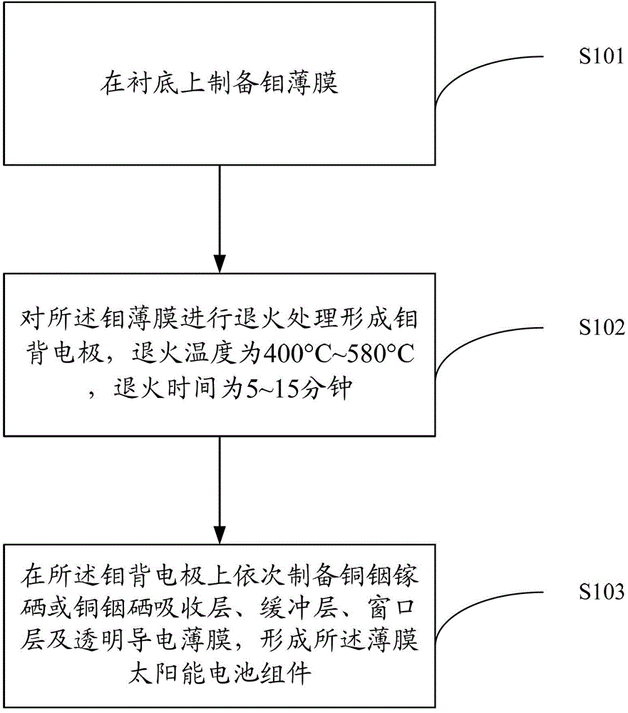
[0027] see figure 1 , the preparation method of the thin-film solar cell assembly of an embodiment, comprises the steps:
[0028] Step S101 , preparing a molybdenum thin film on a substrate.
[0029] The substrate can be glass, such as soda lime glass. The preparation method can be DC magnetron sputtering method, radio frequency magnetron sputtering method, electron beam evaporation method and the like.
[0030] In one embodiment, the cleaned substrate (such as soda lime glass) can be placed in a vacuum with a certain background (such as 1×10 -5 Pa) coating device (such as DC magnetron sputtering chamber). Then adjust the working air flow (such as argon 10sccm), and adjust the air pressure (such as by adjusting the gate valve related to the vacuum pump to make the working pressure of the chamber 1~0.3Pa), adjust the sputtering power (such as 350~1000W), and start the magnetic Controlled sputtering coating. The thickness of the prepared molybdenum film is 0.5-1 μm.
[003...
Embodiment 1
[0039] Fabrication of copper indium selenide (CIS) thin film solar cell modules
[0040] The background vacuum is 1×10 -5 Put clean soda-lime glass in the DC magnetron sputtering chamber of Pa. Adjust the working pressure to 0.3Pa, adjust the power to 350W, and start magnetron sputtering to obtain the first molybdenum layer with a thickness of about 0.5 μm. Adjust the working pressure to 0.05Pa, adjust the power to 500W, and start magnetron sputtering to obtain a second molybdenum layer with a thickness of about 0.5 μm. The first molybdenum layer and the second molybdenum layer constitute a molybdenum thin film with a thickness of 1 μm.
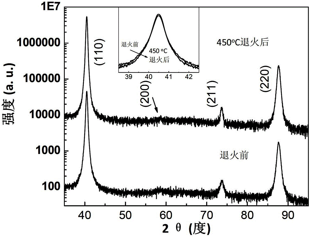
[0041] After sputtering, the molybdenum thin film was transported to the vacuum heating annealing chamber in the vacuum system, and the temperature was raised to 450 ° C in 10 minutes, and after 15 minutes of heat preservation, it was naturally cooled to room temperature. That is to say, a molybdenum thin film suitable for use as a back el...
Embodiment 2
[0053] Fabrication of Copper Indium Gallium Selenide (CIGS) Thin Film Solar Cell Modules
[0054] The background vacuum is 1×10 -5 Put clean soda-lime glass in the DC magnetron sputtering chamber of Pa. Adjust the working pressure to 0.3Pa, adjust the power to 350W, and start magnetron sputtering to obtain the first molybdenum layer with a thickness of about 0.5 μm. Adjust the working pressure to 0.05Pa, adjust the power to 500W, and start magnetron sputtering to obtain a second molybdenum layer with a thickness of about 0.5 μm. The first molybdenum layer and the second molybdenum layer constitute a molybdenum thin film with a thickness of 1 μm.
[0055] After the sputtering is completed, the molybdenum film is transported to the vacuum heating annealing chamber in a vacuum system, and the temperature is raised to 580 ° C in 10 minutes, and after 15 minutes of heat preservation, it is naturally cooled to room temperature. That is to say, a molybdenum thin film suitable for ...
PUM
| Property | Measurement | Unit |
|---|---|---|
| Thickness | aaaaa | aaaaa |
| Thickness | aaaaa | aaaaa |
| Thickness | aaaaa | aaaaa |
Abstract
Description
Claims
Application Information
 - R&D
- Intellectual Property
- Life Sciences
- Materials
- Tech Scout
- Unparalleled Data Quality
- Higher Quality Content
- 60% Fewer Hallucinations
Browse by: Latest US Patents, China's latest patents, Technical Efficacy Thesaurus, Application Domain, Technology Topic, Popular Technical Reports.
© 2025 PatSnap. All rights reserved.Legal|Privacy policy|Modern Slavery Act Transparency Statement|Sitemap|About US| Contact US: help@patsnap.com


