Transparent conductive layer, target for transparent conductive layer and a process for producing the target for transparent conductive layer

A technology of a transparent conductive film and a manufacturing method, which is applied to the conductive layers, oxide conductors, non-metallic conductors and other directions on an insulating carrier, can solve problems such as the influence of component characteristics, and achieve stable resistivity, improved conductivity, and low resistance characteristics. Effect

Inactive Publication Date: 2013-04-10
ADVANCED NANO PROD CO LTD
View PDF9 Cites 4 Cited by
  • Summary
  • Abstract
  • Description
  • Claims
  • Application Information

AI Technical Summary

Problems solved by technology

However, when the above-mentioned ITO thin film is used to fabricate elements, the chan

Method used


Image

  • Transparent conductive layer, target for transparent conductive layer and a process for producing the target for transparent conductive layer
  • Transparent conductive layer, target for transparent conductive layer and a process for producing the target for transparent conductive layer
  • Transparent conductive layer, target for transparent conductive layer and a process for producing the target for transparent conductive layer

Examples


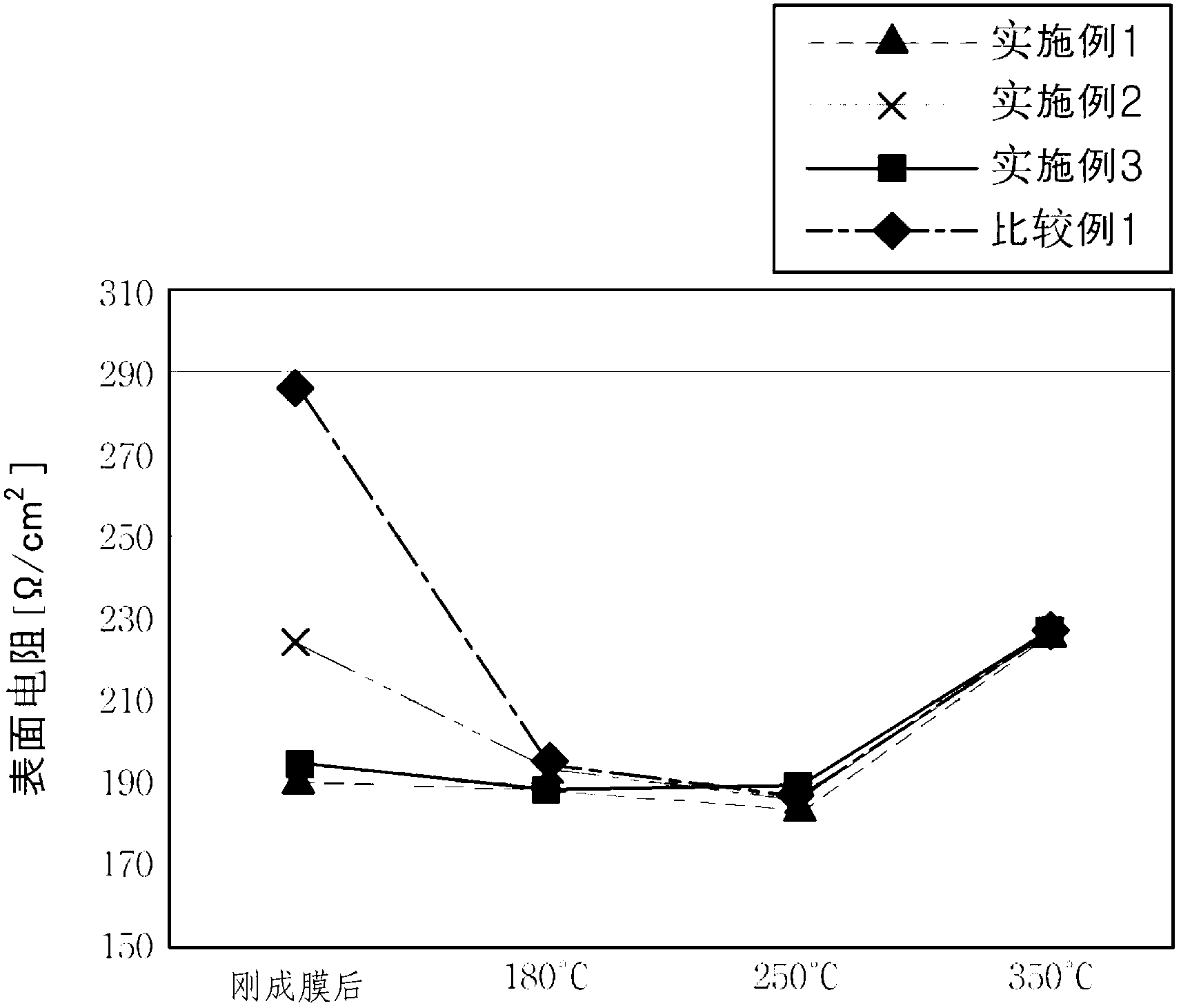
Embodiment 1 to Embodiment 3 and comparative example 1

[0076] Example 1 to Example 3 and Comparative Example 1: Manufacture of sputtering target

Embodiment 1

[0078] Indium nitride (In(NO 3 ) 3 ·6H 2 O) 1730g and green tin (SnCl 4 ·3H 2 After O) 36.5 g was dissolved in 60 ml of ethanol, ultrapure water was added as a pH adjuster and stirred at 50° C. for 12 hours to obtain a solution of pH 3.

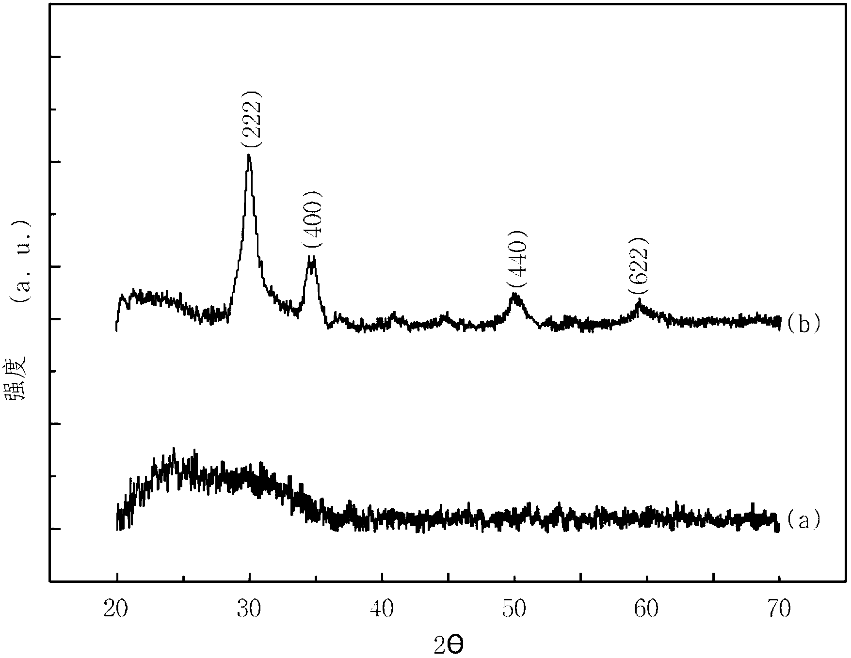
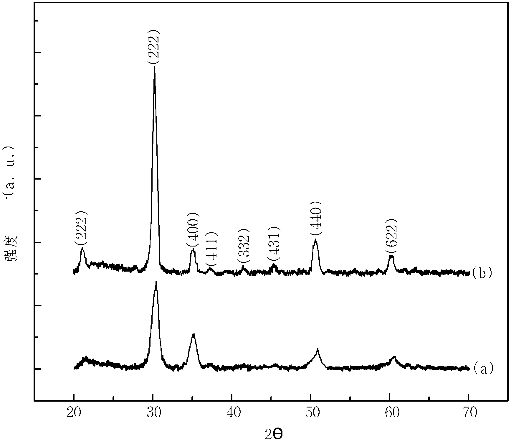
[0079] Next, to the above solution was added NH 4 OH aqueous solution to bring the pH to 9. Thereafter, the reaction was carried out at 40° C. for 20 hours to produce a precipitate. After the above-mentioned precipitate was separated, it was washed three times with ultrapure water, and then dried with hot air at 120° C. to obtain a powder. Afterwards, the above powder was put into an electric furnace and heat-treated (calcined) at a temperature of 750° C. for 2 hours to obtain ITO.

[0080] In addition, the average particle diameter and specific surface area of ​​the above-mentioned ITO are shown in Table 1 below.

[0081] 【Table 1】

[0082]

[0083] Next, 2 g of tantalum oxide and 0.07 g of polyvinyl alcohol were added to 998 g of ...

Embodiment 2

[0090] A sputtering target was prepared in the same manner as in Example 1 except that 5 g of tantalum oxide was added to the above-mentioned ITO995 g. The ICP component inspection results of the above-mentioned sputtering targets showed a weight ratio of Ta:In:Sn=4.902:92.37:2.728. In addition, the density and surface resistivity of the said sputtering target are shown in Table 3 below.

[0091] 【table 3】

[0092]

[0093] Next, the above-mentioned sputtering target was installed in the RF magnetron sputtering machine and the initial vacuum degree in the chamber was adjusted to 1×10 -6 Torr below. Thereafter, an In—Sn—Ta—O-based thin film was deposited on the above-mentioned glass substrate at atmospheric temperature to a thickness of 100 nm.


PUM

PropertyMeasurementUnit
Resistivityaaaaaaaaaa

Abstract

The present invention relates to a transparent conductive layer, which comprises, based on a total weight of the transparent conductive layer, 0.01 - 10 wt% of an additive comprising a compound having at least one or two selected from the group that consists of tantalum, niobium and vanadium; and 90 - 99.99 wt% of an indium tin oxide (ITO).

Description

technical field [0001] The present invention relates to a transparent conductive film, a target for a transparent conductive film, and a method for producing a target for a transparent conductive film. [0002] This application claims the benefit of the filing date of Korean Patent Application No. 10-2010-0052772 filed at the Korean Patent Office, and the entire contents thereof are incorporated in this specification. Background technique [0003] Transparent conductive films are widely used in transparent electrodes, car windows, heat reflecting films for buildings, anti-static films, or anti-fogging for freezer show cases Transparent heating element, etc. [0004] In addition, the above-mentioned transparent electrodes need to have high light transmittance and electrical conductivity. Specifically, the above-mentioned transparent electrode has a light transmittance of more than 85% in the range of visible light, and a resistivity of 1×10 -3 Ω·cm or less is preferable. ...

Claims


Application Information

Patent Timeline
IPC IPC(8): H01B1/02H01B1/08H01B5/14
CPCH01B1/08C23C14/086C23C14/3407H01B5/14
Inventor 朴壮愚金相熙
Owner ADVANCED NANO PROD CO LTD
Why Eureka
Try Eureka