Wear-resistant antimicrobial ABS (acrylonitrile-butadiene-styrene) modified material and preparation method thereof
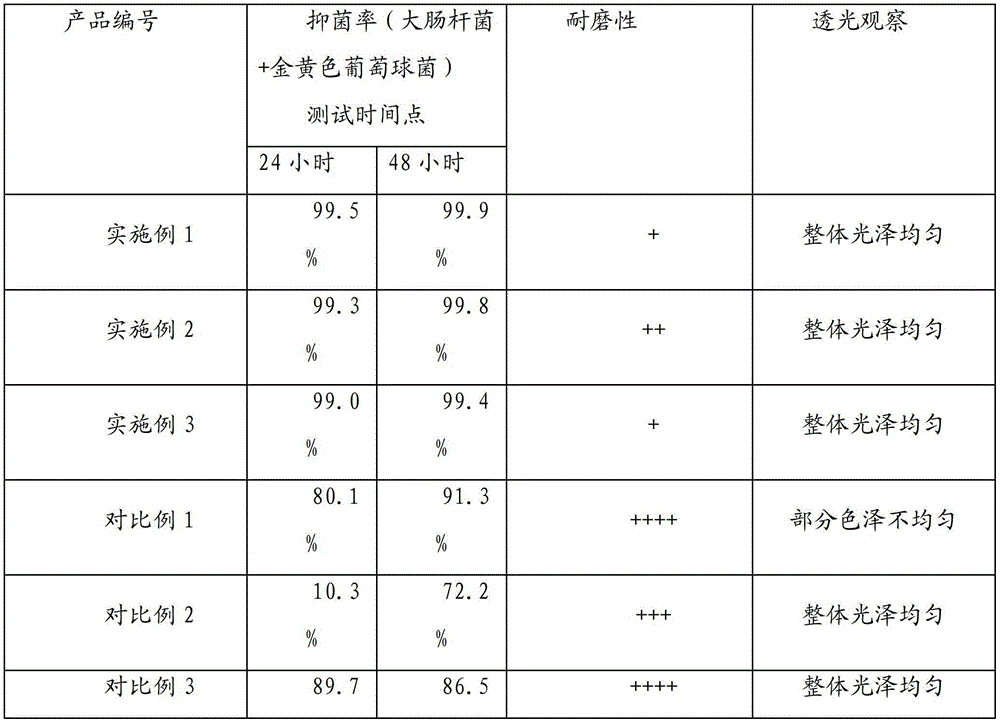
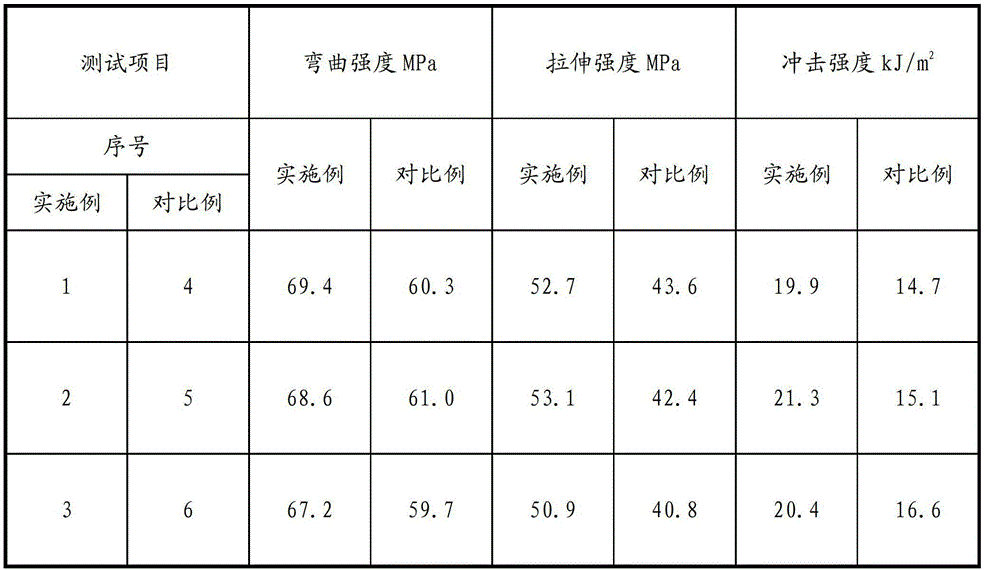
An ABS material and antibacterial material technology, applied in the field of medical materials, can solve the problems of inability to effectively achieve antibacterial, material scratches, insufficient strength, etc., and achieve the effect of preventing crystal agglomeration, enhancing mechanical properties, and uniform and dense film.
- Summary
- Abstract
- Description
- Claims
- Application Information
AI Technical Summary
Problems solved by technology
Method used
Image
Examples
Embodiment 1
[0026] Using the melt blending method to mix 75 parts of PC, 2 parts of nano-titanium dioxide particles, 3 parts of nano-silver particles, 6 parts of ethylene-propylene copolymer, 0.1 parts of antioxidant BHT, 10 parts of MBS and 3.9 parts by weight Parts of styrene-maleic anhydride random copolymer were mixed evenly.
[0027] The above materials are injection molded into a cylindrical shape with an injection molding machine, placed overnight under natural conditions, and then placed in an oxygen-containing gas atmosphere, pure titanium is used as a target, and the plasma sputtering process is performed using an existing plasma coating machine , in the plasma sputtering process, the radio frequency power is 70w, the bias voltage is 50V, and the sputtering time is 15 minutes.
[0028] After sputtering, the thickness of the titanium dioxide film on the surface of the plate is 300nm.
Embodiment 2
[0030] The PC of 80 parts, the nano-titanium dioxide particle of 1.5 parts, the nano-silver particle of 1 part, the alpha olefin oligomer of 4 parts, the antioxidant 168 of 1 part, the MMB of 8 parts and 4.5 parts of styrene-maleic anhydride random copolymer were mixed evenly.
[0031] The above-mentioned materials are blown into a conduit shape by a blow molding machine, placed overnight under natural conditions, and then the conduit is placed in an oxygen-containing gas atmosphere, with pure titanium as the target material, and plasma sputtering is performed using an existing plasma coating machine. In the plasma sputtering process, the radio frequency power is 150w, the bias voltage is 65V, and the sputtering time is 20 minutes.
[0032] After sputtering, the thickness of the titanium dioxide film on the surface of the plate is 450nm.
Embodiment 3
[0034] Using the melt blending method, 86 parts of PC, 1 part of nano-titanium dioxide particles, 0.5 parts of nano-silver particles, 2 parts of ethylene-propylene copolymer, 0.1 part of antioxidant 1010, 8.4 parts of ASA and 2 parts were mixed by weight. Parts of styrene-maleic anhydride random copolymer were mixed evenly.
[0035] The above components are dried until the water content is lower than 0.01 wt%, and the above components are melted and mixed with an internal mixer to prepare an ABS modified material.
[0036] The above materials are molded into sheets by an injection molding machine, placed overnight under natural conditions, and then the sheets are placed in an oxygen-containing gas atmosphere, pure titanium is used as a target, and plasma sputtering is performed using an existing plasma coating machine process, in the plasma sputtering process, the radio frequency power is 200w, the bias voltage is 80V, and the sputtering time is 30 minutes.
[0037] After spu...
PUM
| Property | Measurement | Unit |
|---|---|---|
| particle diameter | aaaaa | aaaaa |
| particle diameter | aaaaa | aaaaa |
| thickness | aaaaa | aaaaa |
Abstract
Description
Claims
Application Information


