The defects of
extreme ultraviolet masks can be divided into two types: amplitude type defects and phase type defects. The amplitude type defects are generally located on the surface of the Mo / Si multilayer film, and the phase type defects are hidden deep inside the Mo / Si multilayer film. Therefore, the phase type defects Defects are more difficult to detect with traditional
microscopy, which also poses challenges for EUV
mask defect detection
The main problem of this solution is that only the structural lines of the wider defects buried under the multilayer film can be detected, while the narrower lines are imaged, and the resulting image is larger than the width of the actual defect lines
Francesco Cerrina and others proposed an indirect detection method in the invention patent "Defect inspection of
extreme ultraviolet lithography masks and the like" (patent number: US7179568 B2), the main principle of which is: extreme
ultraviolet light is irradiated to a blank
mask On the surface, the extreme
ultraviolet light reflected by the blank
mask is incident on an auxiliary detection plate coated with
photoresist. The
photoresist coated on the auxiliary detection plate contains fluorescent dyes. If the detected mask contains phase type or For amplitude defects, due to the scattering of the detection light by the defects, the
exposure of the
photoresist at the position corresponding to the defect on the auxiliary detection plate is insufficient, and the underexposed photoresist cannot be removed in the next development, and the fluorescent excitation
light source is used After irradiating the developed auxiliary detection plate, the
fluorescence emitted by the underexposed photoresist can be observed with an ordinary
microscope, so as to determine the number and location of defects. This method is complicated, time-consuming, and expensive to detect.
Defect size and depth information
In the article "
Microscopy of
extreme ultraviolet lithography masks with 13.2nm tabletop
laser illumination" (
OPTICS LETTERS,34(3):271-273,2009), F.Brizuela et al. proposed a transmission-type zone plate micro-
magnification scheme. The
system uses a
light source with a
wavelength of 13.2nm, and a hollowed-out zone plate concentrating illumination mask. The converging light is incident at an incident angle of 6°, and the
light beam reflected from the mask passes through an off-axis zone plate (0.0625NA) to illuminate the image. Projected directly into the extreme ultraviolet CCD, the
magnification is 660 times. The
disadvantage of this
system is that the energy
utilization rate of the transmission zone plate is low. It is still a traditional imaging method and is not sensitive to phase defects.
Tetsuo Harada et al proposed a mask for coherent scattering imaging in "
Mask observation results using a coherent extreme ultraviolet scattering
microscope at NewSUBARU" (Journal of Vacuum Science & Technology B, 27(6): 3203-3207, 2009) Defect detection system, which adopts the
diffraction conduction theory of mirrorless imaging. By recording the pattern of scattered and diffracted beams, the far-
field pattern can be used to reconstruct the amplitude and phase information of the
electric field intensity and restore the surface morphology of the mask. This system eliminates all Reflectors reduce system cost, but this solution has complex algorithms and unreliable defect information
CHUANG et al. published a four- to eight-piece reflective spherical or Aspherical optical elements constitute a microscopic detection scheme for extreme ultraviolet mask defects. This scheme adds an electronic amplification system on the basis of optical microscopic amplification, so it has certain advantages in overall
magnification and can detect small defects. , but this solution uses multi-reflective extreme ultraviolet optical spherical and aspheric surfaces, which is difficult to process and high in manufacturing costs. At the same time, this solution belongs to the traditional microscopic amplification method and is not sensitive to phase defects.
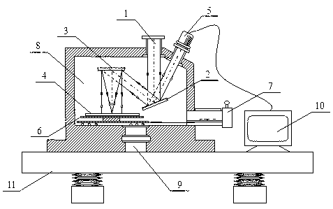
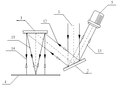
Gao Zhishan, Wang Shuai and others invented a bifocal zone plate-based interference in the invention patent "Double-focal oblique-incidence
interference microscopy device for
extreme ultraviolet lithography mask defect detection" (application number: 201310069314.2) The microscopic device, which works under the extreme
ultraviolet light of 13.5nm, uses the oblique-incidence interference microscopic characteristics of the bifocal zone plate to transfer the phase-type defect information in the EUV mask to the interferogram, and at the same
time transfer the amplitude-type defect information to the interferogram. The defect or the physical deformation caused by it is enlarged and imaged, and the defect in the EUV mask is detected by solving the interferogram and identifying the
microscopic image. The device uses reflective and diffractive optical elements. Compared with the multi-
chip reflective system, The number of extreme ultraviolet reflective elements is reduced, it is sensitive to EUV mask phase defects, the
algorithm is simple, and the reliability is high. However, the system uses two double-curvature surface mirrors and two bifocal zone plate interference
microscope objectives. The angle requirements between the four mirrors are high, and the installation and adjustment of the system is difficult, and the device adopts
oblique incidence and defocused lighting, which is limited in defect positioning accuracy and resolution.

