Cu film annealing based method for preparing large-area graphene on SiC substrate

A graphene, large-area technology, applied in the field of microelectronics, can solve the problems of unstable carrier mobility, inability to use large-scale production, small graphene area, etc., to achieve easy control of the growth process, high uniformity, and surface. smooth effect

Inactive Publication Date: 2013-07-03
XIDIAN UNIV
View PDF4 Cites 5 Cited by
  • Summary
  • Abstract
  • Description
  • Claims
  • Application Information

AI Technical Summary

Problems solved by technology

[0009] The purpose of the present invention is to address the above-mentioned deficiencies in the prior art, and propose a method for preparing large-area graphene on a SiC substrate based on Cu film annealing, so as to solve the problem that the graphene prepared by the prior art has a small area and cannot be used for large-scale production , the number of layers is uneven, there are many defects, and the carrier mobility is unstable

Method used


Image

  • Cu film annealing based method for preparing large-area graphene on SiC substrate
  • Cu film annealing based method for preparing large-area graphene on SiC substrate

Examples


Embodiment 1

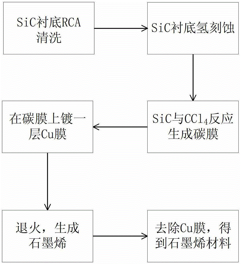
[0027] Example 1, making 4H-SiC and CCl 4 Reaction and Cu film annealing of large-area graphene.

[0028] Step 1: The 4H-SiC substrate is cleaned by the RCA method to remove organic and inorganic chemical pollutants on the sample surface:

[0029] (1.1) Place the 4H-SiC substrate in deionized water for ultrasonic cleaning for 15 minutes, take it out, and rinse it repeatedly with deionized water;

[0030] (1.2) Soak the cleaned 4H-SiC substrate in a solution of ammonia water: hydrogen peroxide: deionized water = 1:2:5, boil it, soak it for 15 minutes, and wash it repeatedly with deionized water for the second time;

[0031] (1.3) The 4H-SiC substrate after the second cleaning was immersed in a solution of hydrochloric acid:hydrogen peroxide:deionized water=1:2:8, boiled, soaked for 15min, and washed repeatedly with deionized water for the third time.

[0032] Step 2: performing hydrogen etching on the 4H-SiC substrate after RCA cleaning.

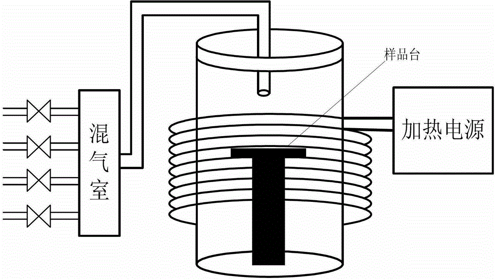
[0033] Set the pressure in the reac...

Embodiment 2

[0045] Embodiment 2, making 4H-SiC and CCl 4 Reaction and Cu film annealing of large-area graphene.

[0046] Step 1: RCA is used to clean the 4H-SiC substrate to remove organic and inorganic chemical pollutants on the surface of the sample. The cleaning steps are the same as in Example 1.

[0047] Step 2: Put the 4H-SiC sample into the quartz tube, and heat it with exhaust gas.

[0048] Set the pressure in the reaction chamber to 13.3Pa, raise the temperature to 1600°C, and perform hydrogen etching on the substrate for 30 minutes. The hydrogen flow rate is 100L / min to remove scratches on the surface of the 4H-SiC substrate and generate nanometer-level high periodicity. Smooth step topography.

[0049] Step 3: removing hydrogen etching residual compounds on the surface of the 4H-SiC substrate.

[0050] Lower the temperature of the reaction chamber to 850°C and feed SiH 4 The gas, whose flow rate is 0.5ml / min, lasts for 10min to remove the compound produced by hydrogen etchi...

Embodiment 3

[0058] Embodiment 3, making 6H-SiC and CCl 4 Reaction and Cu film annealing of large-area graphene.

[0059] Step A: Cleaning the 6H-SiC substrate by using the RCA method, and the cleaning steps are the same as in Embodiment 1.

[0060] Step B: Set the pressure in the reaction chamber to 13.3Pa, raise the temperature to 1600°C, and perform hydrogen etching on the substrate for 20 minutes with a hydrogen flow rate of 120L / min to remove scratches on the surface of the 6H-SiC substrate and produce nanoscale high The periodic smooth step morphology.

[0061] Step C: Lower the temperature of the reaction chamber to 850°C and feed SiH 4 The gas, whose flow rate is 0.5ml / min, lasts for 10min to remove the compound produced by hydrogen etching on the surface of the 6H-SiC substrate.

[0062] Step D: Heat the reaction chamber to 1000°C, open the gas valve, and put Ar gas and CCl 4 After the gas is passed into the gas mixing chamber and mixed, it is passed into the reaction chamber,...


PUM


Abstract

The invention discloses a Cu film annealing based method for preparing large-area graphene on an SiC substrate, and mainly solves problems of poor continuity, high porosity and uneven layers of graphene prepared in the prior art. The method comprises the steps as follows: firstly, cleaning an SiC sample with an RCA cleaning method; secondly, performing hydrogen etching on the cleaned SiC sample; thirdly, feeding Ar gas and CCl4 gas into a gas mixing chamber for mixing, feeding the mixed gas into a reaction chamber, and enabling the CCl4 gas and the SiC to react and generate a carbon film; fourthly, plating a Cu film on the generated carbon film; fifthly, placing the sample plated with the Cu film in the Ar gas, annealing the sample at the temperature ranging from 900 DEG C to 1100 DEG C for 15 to 25 minutes, and enabling the carbon film to reconstruct the graphene; and sixthly, removing the Cu film from the graphene sample. The method has the advantages of good continuity and evenness and low porosity of the graphene and can be used in various fields of biology, optics, electricity, sensors and the like.

Description

technical field [0001] The invention belongs to the technical field of microelectronics, and relates to a semiconductor film material and a preparation method thereof, in particular to a method for preparing large-area graphene on a SiC substrate based on Cu film annealing. technical background [0002] With the announcement of the winner of the Nobel Prize in Physics in 2010, Graphene has also become the focus of discussion. In 2004, Andre Geim and Konstantin Novoselov of the University of Manchester successfully peeled off graphene from graphite using ordinary adhesive tape. This material is only one carbon atom thick and is currently known the thinnest material. Not only is it the thinnest known material, it's also very strong and flexible; as a single substance, it transports electrons faster than any known conductor at room temperature. Graphene can be applied to the fields of transistors, touch screens, and gene sequencing, and it is expected to help physicists make ...

Claims


Application Information

Patent Timeline
Patent Type & Authority Applications(China)
IPC IPC(8): C01B31/04C01B32/188
Inventor 郭辉张晨旭张玉明刘杰雷天民
Owner XIDIAN UNIV
Why Eureka
Try Eureka