N-type MOS field-effect transistor and formation method thereof, semiconductor device and formation method of semiconductor device

A field effect tube and semiconductor technology, applied in the direction of semiconductor devices, semiconductor/solid state device manufacturing, electrical components, etc., can solve the problems of reducing the operating speed of integrated circuits, reducing the frequency of semiconductor device inverters, and n-type MOS field effect tubes Capacitance is too large to achieve the effect of increasing frequency, reducing overlapping capacitance, and reducing capacitance

Active Publication Date: 2013-07-03
SEMICON MFG INT (SHANGHAI) CORP +1
View PDF8 Cites 12 Cited by
  • Summary
  • Abstract
  • Description
  • Claims
  • Application Information

AI Technical Summary

Problems solved by technology

[0007] However, the overlap capacitance (overlap capacitance) of the n-type MOS field effect transistor formed by the prior art is too large, resulting in a relatively large capacitance of the n-type MOS field effect transistor, so that the semiconductor device composed of the n-type MOS field effect transistor For example, the frequency of the inverter is reduced, reducing the operating speed of the integrated circuit

Method used


Image

  • N-type MOS field-effect transistor and formation method thereof, semiconductor device and formation method of semiconductor device
  • N-type MOS field-effect transistor and formation method thereof, semiconductor device and formation method of semiconductor device
  • N-type MOS field-effect transistor and formation method thereof, semiconductor device and formation method of semiconductor device

Examples


specific Embodiment 1

[0083] Figure 3 to Figure 8 It is a schematic cross-sectional structure diagram of the method for forming an n-type MOS field effect transistor according to Embodiment 1 of the present invention.

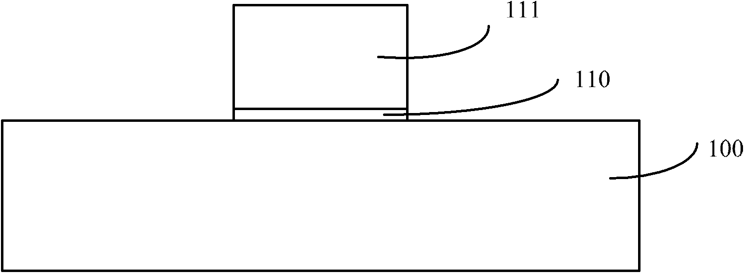
[0084] Please refer to image 3 A semiconductor substrate 100 is provided, and a gate dielectric layer 110 and a gate 111 are sequentially formed on the surface of the semiconductor substrate 100 .

[0085] The semiconductor substrate 100 may be made of silicon, germanium, gallium arsenide, silicon germanium or silicon-on-insulator, and p-type doping is performed in the semiconductor substrate 100 .

[0086] The formation process of the gate dielectric layer 110 and the gate 111 is as follows: a dielectric layer and a gate layer are sequentially formed on the surface of the semiconductor substrate 100, a photoresist is coated on the surface of the gate layer and patterned by exposure and development. To mask and etch the dielectric layer and the gate layer, remove the photoresist...

specific Embodiment 2

[0111] The method for forming the n-type MOS field effect transistor of the present invention will be described below in conjunction with the second embodiment.

[0112] Figure 9 , Figure 10 It is a schematic cross-sectional structure diagram of a method for forming an n-type MOS field effect transistor according to Embodiment 2 of the present invention.

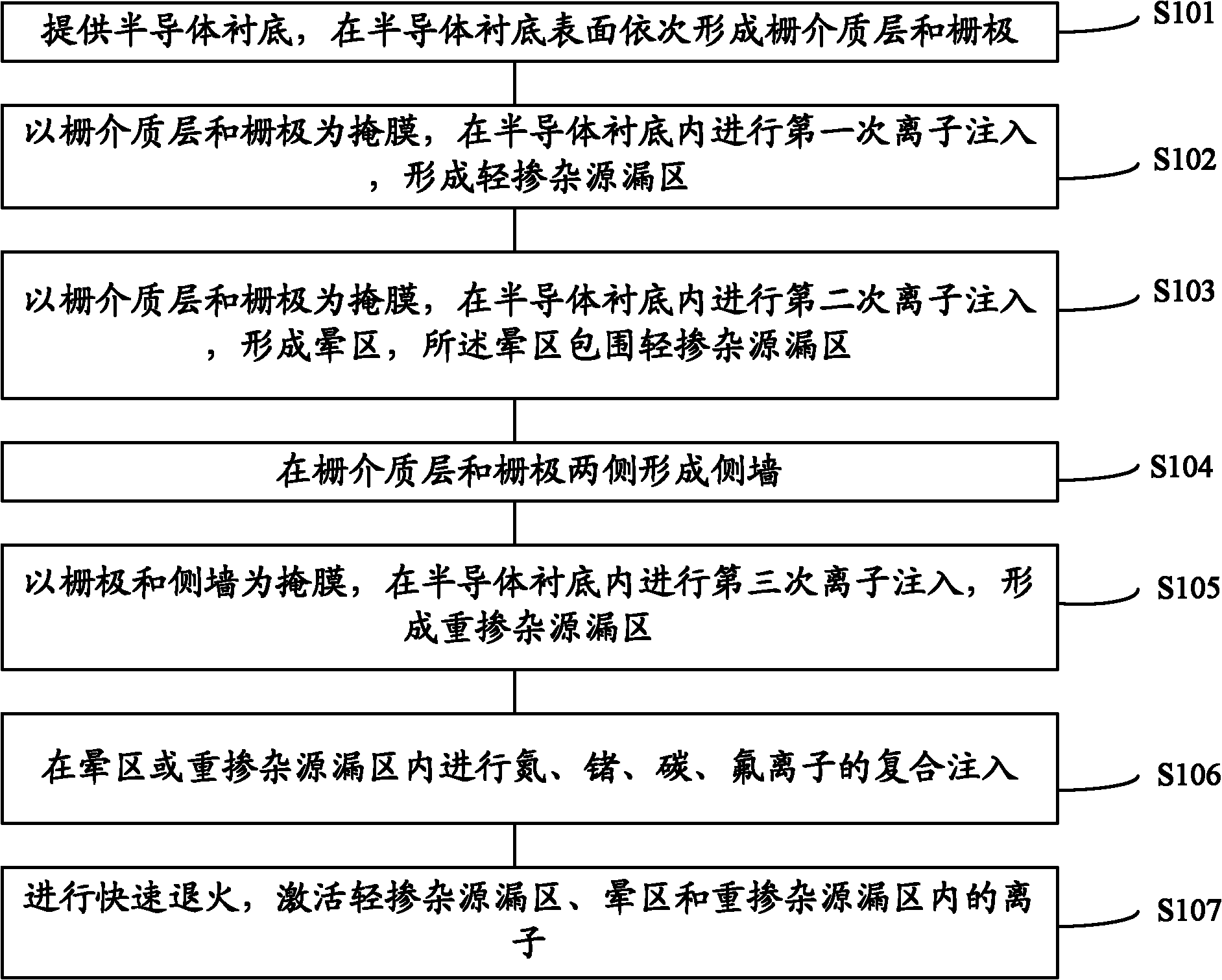
[0113] Please refer to Figure 9 , providing a semiconductor substrate 300, sequentially forming a gate dielectric layer 310 and a gate 311 on the surface of the semiconductor substrate 300; using the gate dielectric layer 310 and the gate 311 as a mask, performing the first ion implantation in the semiconductor substrate 300 to form The lightly doped source and drain regions, and the second ion implantation form a halo region, and the halo region surrounds the lightly doped source and drain regions; perform rapid annealing to activate the ions in the lightly doped source and drain regions and the halo region, and the ac...

specific Embodiment 3

[0139] Figure 12 to Figure 18 It is a schematic cross-sectional structure diagram of a method for forming a semiconductor device according to Embodiment 3 of the present invention.

[0140] Please refer to Figure 12 , providing a semiconductor substrate 200, the semiconductor substrate has an n-type MOS field effect transistor region 201 and a p-type MOS field effect transistor region 202, and a gate dielectric layer 220 and a gate 221 are sequentially formed on the surface of the n-type MOS field effect transistor region 201 , forming a gate dielectric layer 222 and a gate 223 on the surface of the p-type MOS field effect transistor region 202 .

[0141] The n-type MOS field effect transistor region 201 and the p-type MOS field effect transistor region 202 are isolated by a shallow trench isolation structure 240 .

[0142] The semiconductor substrate 200 may be silicon, germanium, gallium arsenide, silicon germanium or silicon-on-insulator, p-type doping is performed on t...


PUM


Abstract

The invention provides an n-type MOS (metal oxide semiconductor) field-effect transistor and a formation method thereof, a semiconductor device and a formation method of the semiconductor device. The formation method of the n-type MOS field-effect transistor comprises the steps that a semiconductor substrate is provided; a grid medium layer and a grid electrode are formed on the surface of the semiconductor substrate sequentially, and serve as masking films; first ion implantation is conducted in the semiconductor substrate; lightly doped source drain regions are formed; the grid medium layer and the grid electrode serve as the masking films; second ion implantation is conducted in the semiconductor substrate; halo regions are formed, and surround the lightly doped source drain regions; side walls are formed on the two sides of the grid medium layer and the grid electrode; the grid electrode and the side walls serve as masking films; third ion implantation is conducted in the semiconductor substrate; heavily doped source drain regions are formed; composite implantation of nitrogen, germanium, carbon and fluorine ions is conducted in the halo regions or the heavily doped source drain regions; rapid annealing is conducted; and the ions in the lightly doped source drain regions, the halo regions and the heavily doped source drain regions are activated. Overlap capacitance of the formed n-type MOS field-effect transistor is reduced.

Description

technical field [0001] The invention relates to the technical field of semiconductor manufacturing, in particular to an n-type MOS field effect transistor used for an inverter and a forming method thereof, a semiconductor device and a forming method thereof. Background technique [0002] Ring Oscillator (Ring Oscillator, referred to as RO) is a semiconductor device that is widely used in integrated circuits to provide clock signals for various digital signal processing modules, so the frequency of the ring oscillator determines the operating speed of the integrated circuit , is an important semiconductor device that affects the performance of integrated circuits. [0003] The ring oscillator consists of an odd number of inverters in series to form a loop, and the frequency of the ring oscillator is: f=1 / (T d *N), where T d is the delay time of a single inverter, N is the number of inverters in the series loop, it can be seen that in order to increase the frequency of the r...

Claims


Application Information

Patent Timeline
Patent Type & Authority Applications(China)
IPC IPC(8): H01L21/336H01L21/265H01L29/78H01L29/08H01L21/8238
Inventor 李勇居建华
Owner SEMICON MFG INT (SHANGHAI) CORP
Why Eureka
Try Eureka