Manufacturing method for crystalline silicon solar MWT (metallization wrap-through) cell and manufactured cell

A manufacturing method and solar energy technology, applied in the field of solar cells, can solve the problem that it is difficult to achieve high aspect ratio in one printing, and achieve the effects of reducing optical loss, increasing short-circuit current, and easy operation

Inactive Publication Date: 2013-07-03
EGING PHOTOVOLTAIC TECHNOLOGY CO LTD
View PDF8 Cites 11 Cited by
  • Summary
  • Abstract
  • Description
  • Claims
  • Application Information

AI Technical Summary

Problems solved by technology

[0007] In the screen printing process, the smaller the printed width and the higher the height within a certain range, the higher the photoelectric conversion efficiency of the battery. However, it is difficult to achieve the ideal aspect ratio in one printing of the traditional process.

Method used


Image

  • Manufacturing method for crystalline silicon solar MWT (metallization wrap-through) cell and manufactured cell
  • Manufacturing method for crystalline silicon solar MWT (metallization wrap-through) cell and manufactured cell
  • Manufacturing method for crystalline silicon solar MWT (metallization wrap-through) cell and manufactured cell

Examples


Embodiment 1

[0035] This embodiment is a method for manufacturing a crystalline silicon solar MWT cell, comprising the following steps:

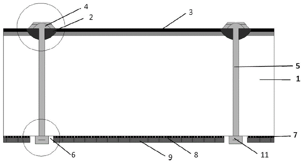
[0036] (a) Using a P-type single crystal or polycrystalline silicon substrate 1, using a laser to make conductive through holes 5 on the crystalline silicon substrate, the cross-sectional shape is cylindrical, the number is 4×4, and the hole size is 50-600 μm;

[0037] (b) Wet texturing of perforated crystalline silicon substrates using chemical solutions;

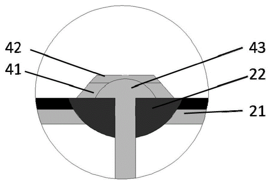
[0038] (c) Use a polyester screen to print the light-receiving surface of the perforated crystalline silicon substrate with phosphor paste in the grid line area, form a heavily doped area 22 in the printed grid line area, and form a lightly doped area in the unprinted non-grid line area In area 21, the printing line width of phosphorous paste is 20-500 μm;

[0039] (d) Phosphorus diffusion using a liquid phosphorus source;

[0040] (e) Etching the edge of the silicon substrate and performing de-PS...

Embodiment 2

[0048]The difference between Embodiment 2 and Embodiment 1 is that the printing silver paste in step (h) adopts a secondary printing technology, specifically: printing silver paste on the heavily doped region 22 obtained in step (c) to form The light-receiving surface electrode grid line can form a selective emitter structure 2; specifically, the fine grid 41 is printed for the first time in the heavily doped region 22, and the second printing is performed on the first printed fine grid 41 area after drying. Print the fine grid 42 for the second time, and print the front connection area 43 of the fine grid and the conductive hole at the same time; or print the fine grid 41 and the front connection area 43 of the grid line and the conductive hole for the first time in the heavily doped region 22, and then print the first time after drying. Print the fine grid 41 area for the second time to print the fine grid 42, thereby forming the secondary printing structure 4, and a solar ce...

Embodiment 3

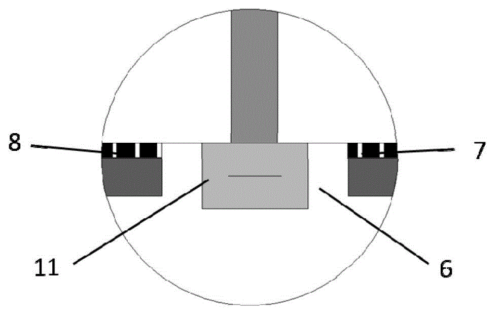
[0051] The difference between Embodiment 3 and Embodiment 1 is that a back passivation process is added between step (e) and step (g), specifically: aluminum oxide and silicon nitride are plated on the backlight surface for back passivation. Passivation, the passivation film 8 on the backlight surface is one or more of silicon nitride film, silicon oxide film and aluminum oxide film, the thickness of the passivation film 8 is 1-100nm; Utilize the laser to engrave the back passivation layer Groove, the width of the rear passivation layer groove 7 is 0.1-1000 μm;

[0052] Such as Figure 1~4 As shown, the crystalline silicon solar MWT cell obtained by the manufacturing method in Example 3 has a structure that the electrode grid line on the light-receiving surface is a selective emission level structure 2, and there is a back passivation layer on the back side, and the back passivation layer is formed by the back passivation layer. The chemical film 8 and the rear passivation la...


PUM

PropertyMeasurementUnit
pore sizeaaaaaaaaaa
thicknessaaaaaaaaaa
widthaaaaaaaaaa

Abstract

The invention discloses a manufacturing method for a crystalline silicon solar MWT (metallization wrap-through) cell. The manufacturing method for the crystalline silicon solar MWT cell comprises the following steps of: producing a conductive through hole; performing wet-method texturization; performing grid line area phosphorous paste printing on a light-receiving surface; diffusing phosphorous; etching the edge of a silicon matrix, and performing PSG (phosphosilicate glass) removal treatment; coating an antireflection film, and printing an emitting electrode contact electrode, a back electrode contact electrode and a base electrode contact electrode; printing the electrode grid line of the light-receiving surface; sintering to form ohmic contact; and electrically insulating the base electrode contact electrode from the emitting electrode contact electrode, so as to finish production for the solar cell. According to the manufacturing method disclosed by the invention, a selective emitting electrode structure is realized on the MWT solar cell; and optical loss is effectively reduced, minority carrier recombination is reduced, various electrode-related resistance losses are reduced, and the short-circuit current ISC, the open-circuit voltage UOC and the filling factor of the cell are remarkable increased by combining with a back passivation technology and a secondary printing technology. The preparation process is easy to operate, capable of being completely compatible with the solar cell production line which is widely applied at present, and suitable for large-scale production.

Description

technical field [0001] The invention belongs to the field of solar cells, and in particular relates to a method for manufacturing a crystalline silicon solar metal wound through hole (MWT) solar cell and a cell manufactured therefrom. Background technique [0002] Facing the increasingly serious global energy crisis and environmental protection issues, crystalline silicon solar photovoltaic power generation as a clean energy source has become an inevitable choice. In order to pursue the cost of photovoltaic power generation to compete with the cost of traditional thermal power generation, improving efficiency and reducing cost has become the goal of the photovoltaic industry, and improving the conversion efficiency of cells in the solar cell manufacturing process is the most important measure. [0003] At present, due to factors such as optical loss, electron-hole recombination, and various resistance losses related to electrodes, there is still a lot of room for improvement...

Claims


Application Information

Patent Timeline
Patent Type & Authority Applications(China)
IPC IPC(8): H01L31/18H01L31/0224H01L31/042H01L31/068
CPCY02E10/547Y02P70/50
Inventor 谢合义李钟华
Owner EGING PHOTOVOLTAIC TECHNOLOGY CO LTD
Why Eureka
Try Eureka