Ultraviolet photo-detector with nano heterogeneous composite structure and preparation method thereof
A composite structure and nanostructure technology, which is applied in the field of ultraviolet photodetectors and its preparation, can solve problems such as work stability and lifetime impact, severe carrier recombination, and reduced photosensitivity, so as to speed up carrier separation and reduce Composite, good radiation resistance and stability effect
- Summary
- Abstract
- Description
- Claims
- Application Information
AI Technical Summary
Problems solved by technology
Method used
Image
Examples
Embodiment 1
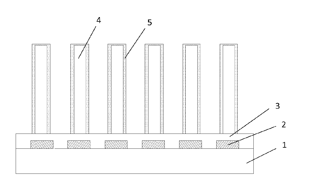
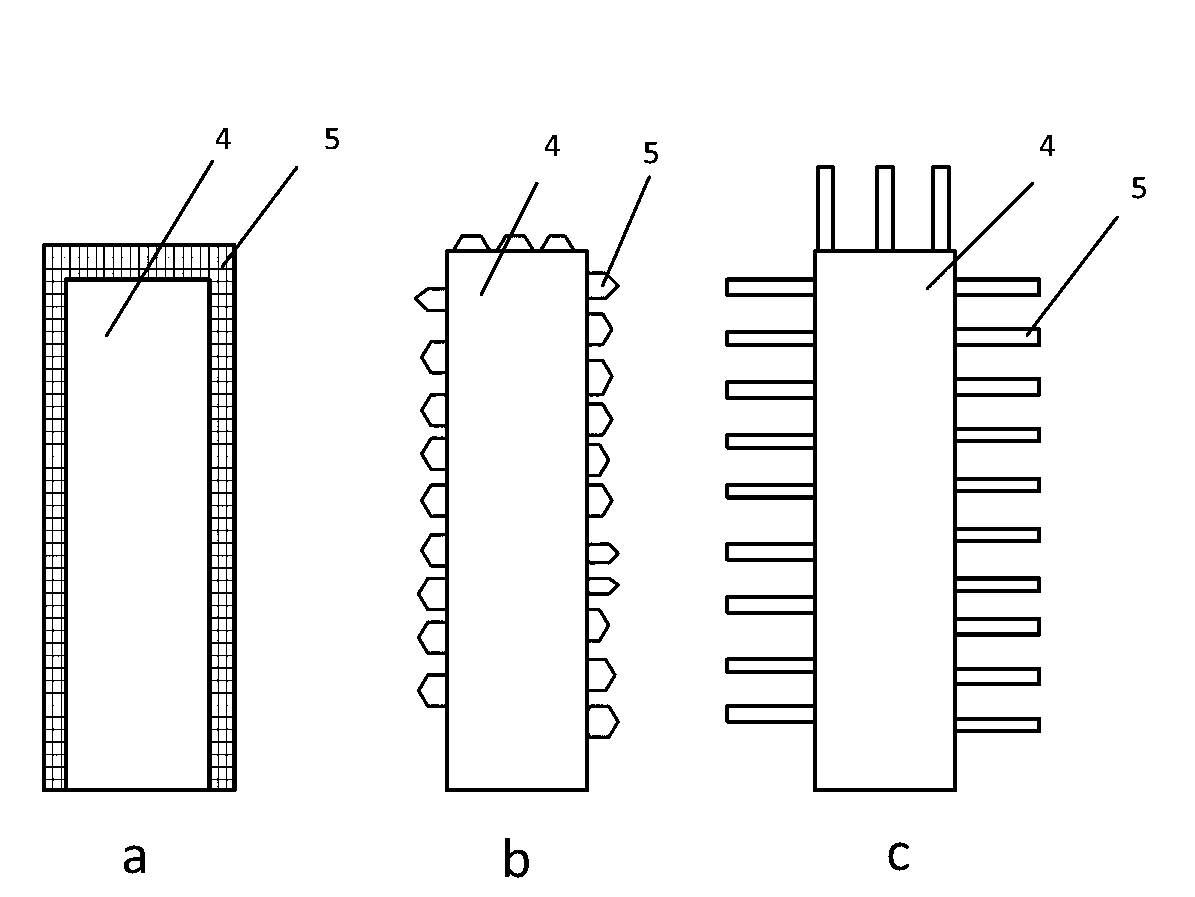
[0042] According to the method described in this example, the following figure 2 with image 3 (a) The UV detector structure shown, in which ZnO nanorods are wrapped with a layer of TiO2 thin film. Its concrete preparation steps are as follows:
[0043] (1) Select a suitable size glass or silicon wafer, clean it, spin-coat PR1000 photoresist on its surface, and pass the photolithography process. figure 1 The photoresist at the position of the middle interdigitated electrode is washed off after exposure to form grooves.
[0044] (2) Deposit a layer of metal nano film on the surface of the above sample by magnetron sputtering or electron beam evaporation process, the thickness of which is preferably 10 nm.
[0045] (3) Soak the above sample in acetone (for example, 30 min) to remove the photoresist.
[0046] (4) Protect the metal junction plate on the right side of the sample with photoresist.
[0047] (5) Coating a layer of ZnO thin film on the surface of the above sample b...
Embodiment 2
[0053] According to the method described in this example, the following figure 2 and image 3 (b) The UV detector structure shown, in which ZnO nanorods are coated with a layer of TiO 2 nanoparticles. Its concrete preparation steps are as follows:
[0054] (1) Choose PET plastic or PDMS of appropriate size, clean it, spin-coat PR1000 photoresist on its surface, and pass the photolithography process. figure 1 The photoresist at the position of the middle interdigitated electrode is washed off after exposure to form grooves.
[0055] (2) Deposit a layer of metal nano film on the surface of the above sample by magnetron sputtering or electron beam evaporation process, the thickness of which is preferably 100nm.
[0056] (3) Soak the above sample in acetone preferably for 30 minutes to remove the photoresist.
[0057] (4) Protect the metal junction plate on the right side of the sample with photoresist.
[0058] (5) Coating a layer of ZnO thin film on the surface of the abo...
Embodiment 3
[0063] According to the method described in this example, the following figure 2 and image 3 (c) The UV detector structure shown, in which ZnO nanorods are coated with a layer of TiO 2 Nano stave. Its concrete preparation steps are as follows:
[0064] (1) Select a suitable size glass or silicon wafer, clean it, spin-coat PR1000 photoresist on its surface, and pass the photolithography process. figure 1 The photoresist at the position of the middle interdigitated electrode is washed off after exposure to form grooves.
[0065] (2) Deposit a layer of metal nano film on the surface of the above sample by magnetron sputtering or electron beam evaporation process, the thickness of which is preferably 200nm.
[0066] (3) Soak the above samples in acetone for 30 minutes to remove the photoresist.
[0067] (4) Protect the metal junction plate on the right side of the sample with photoresist.
[0068] (5) Coating a layer of ZnO thin film on the surface of the above sample by m...
PUM
| Property | Measurement | Unit |
|---|---|---|
| Diameter | aaaaa | aaaaa |
| Height | aaaaa | aaaaa |
| Interdigital spacing | aaaaa | aaaaa |
Abstract
Description
Claims
Application Information


