Method for manufacturing micro-nano graph on sapphire substrate

A sapphire substrate, micro-nano technology, applied in the field of semiconductors, can solve the problems of expensive equipment, high cost, difficulty in achieving nanometer precision, etc., and achieve the effect of improving crystal quality and optical efficiency

Inactive Publication Date: 2013-09-18
INST OF SEMICONDUCTORS - CHINESE ACAD OF SCI
View PDF6 Cites 19 Cited by
  • Summary
  • Abstract
  • Description
  • Claims
  • Application Information

AI Technical Summary

Problems solved by technology

However, the precision of ordinary lithography technology is usually 2-5 microns, and it is difficult to achieve nanometer precision.
At present, the commonly used technologies such as electron beam exposure and nanoimprinting with micro-nano precision require expensive equipment and high costs.

Method used


Image

  • Method for manufacturing micro-nano graph on sapphire substrate
  • Method for manufacturing micro-nano graph on sapphire substrate
  • Method for manufacturing micro-nano graph on sapphire substrate

Examples


Embodiment Construction

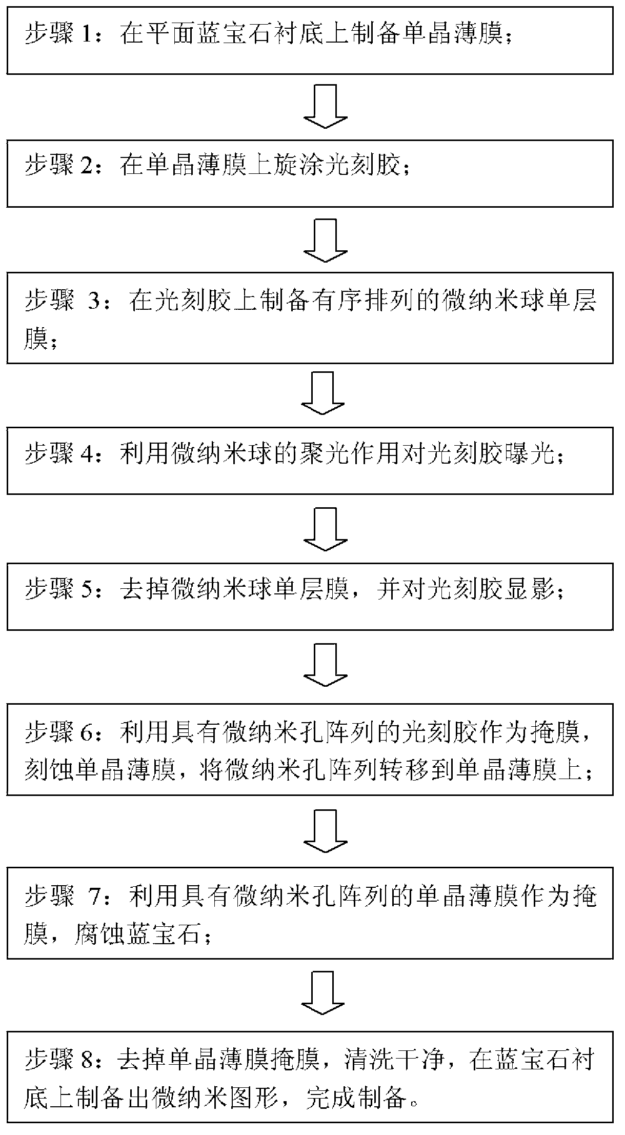
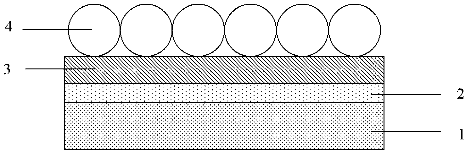
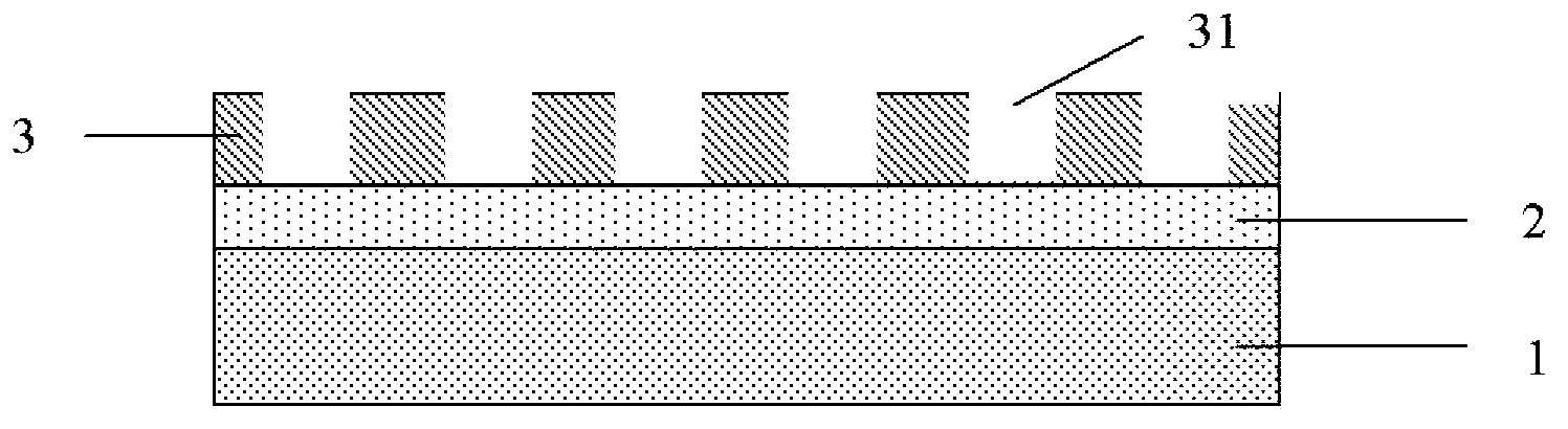
[0018] Please refer to figure 1 , and see in conjunction with Figure 2 to Figure 6 Shown, the present invention provides a kind of method preparing micro-nano pattern on sapphire substrate, comprises the following steps:

[0019] Step 1: prepare a single crystal film 2 on a sapphire substrate 1, the sapphire substrate 1 is a planar sapphire substrate, the size is not limited, the shape is not limited; the material of the single crystal film 2 is silicon dioxide, nitrogen One, two or more of silicon carbide or silicon carbide, can be one layer, two layers or multiple layers, its thickness is 10nm-10000nm, its preferred thickness is 100nm-500nm, its preparation method can adopt plasma enhanced Preparation methods such as vapor deposition, electron beam evaporation or magnetron sputtering.

[0020] Step 2: Spin-coat a layer of photoresist 3 on the single crystal film 2, the photoresist 3 is a positive photoresist with a thickness of 100nm-5000nm, preferably 200nm-2000nm; the t...


PUM

PropertyMeasurementUnit
thicknessaaaaaaaaaa
thicknessaaaaaaaaaa
diameteraaaaaaaaaa

Abstract

A method for manufacturing a micro-nano graph on a sapphire substrate comprises the steps of S1, manufacturing a monocrystal film on the sapphire substrate; S2, rotationally coating a layer of photoresist on the monocrystal film; S3, preparing a sequentially arrayed micro-nano ball monolayer film on the photoresist; S4, carrying out exposure on the photoresist by a photoetching machine by the light condensing function of micro-nano balls; S5, removing the micro-nano ball monolayer film and developing the sequentially arrayed photoresist micro-nano hole array; S6, transferring the micro-nano hole array onto the monocrystal film by a dry etching method to form the monocrystal film micro-nano hole array on the monocrystal film; S7, taking the monocrystal film micro-nano hole array as a mask for wet etching the sapphire substrate, thus obtaining sequential micro-nano graph array on the sapphire substrate; and S8, finishing the manufacturing after the monocrystal film mask is removed.

Description

technical field [0001] The invention belongs to the technical field of semiconductors, in particular to a method for preparing micro-nano patterns on a sapphire substrate. Background technique [0002] Currently, III-V nitride compound semiconductors, such as gallium nitride (GaN), aluminum nitride (AlN), indium nitride (InN), aluminum gallium nitride (AlGaN), indium gallium nitride (InGaN), Aluminum indium nitride (AlInN), aluminum gallium indium nitride (AlInGaN), etc. have a wide range of applications in the fields of ultraviolet / blue / green light-emitting diodes, lasers, photodetectors, solar cells, and power electronic devices. Sapphire substrate has become the most widely used substrate for nitride epitaxial growth due to its low cost. However, due to the heterogeneous epitaxy, the sapphire substrate and the nitride epitaxial layer have a large lattice fit and thermal expansion fit, so the higher stress and higher dislocation density in the nitride epitaxial layer grea...

Claims


Application Information

Patent Timeline
Patent Type & Authority Applications(China)
IPC IPC(8): H01L21/02G03F7/00B82Y40/00
Inventor 董鹏王军喜闫建昌张韵曾建平孙莉莉李晋闽
Owner INST OF SEMICONDUCTORS - CHINESE ACAD OF SCI
Why Eureka
Try Eureka