Stack-based copper zinc tin sulfur selenide (CZTSSe) thin film solar cell and manufacturing method thereof
A copper-zinc-tin-selenium-sulfur and solar cell technology, applied in circuits, photovoltaic power generation, electrical components, etc., can solve the problems of reducing absorption rate and inability to effectively absorb short-wavelength light, and achieve the effect of reducing contact resistance
- Summary
- Abstract
- Description
- Claims
- Application Information
AI Technical Summary
Problems solved by technology
Method used
Image
Examples
Embodiment 1
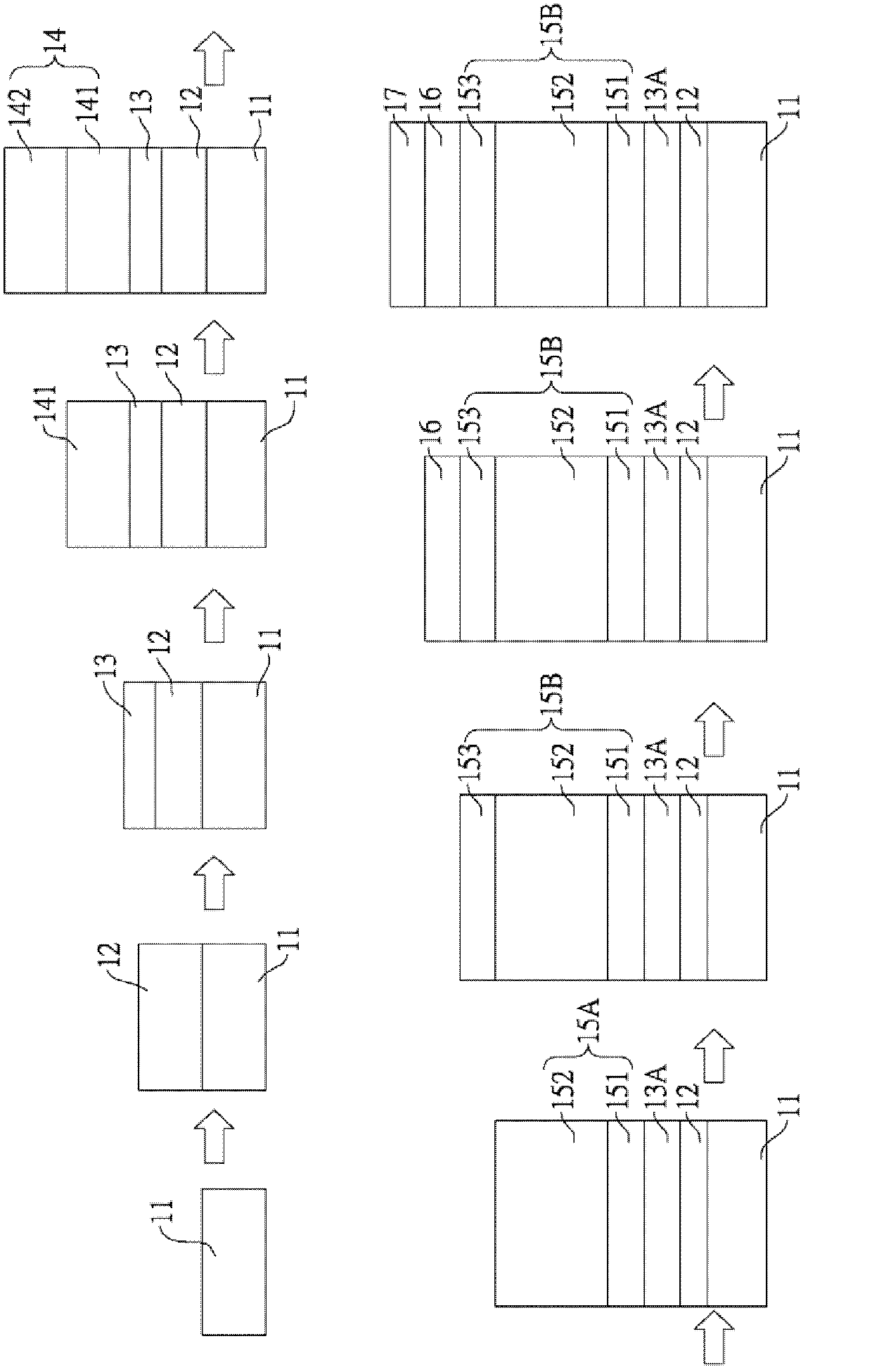
[0050] Below, will match figure 1 As shown, the manufacturing process of the present invention for manufacturing stacked copper-zinc-tin-selenide-sulfur thin film solar cells is described in detail.
[0051] First, a clean substrate 11 is provided. A back electrode layer 12 is formed on the substrate 11 by a sputtering process. In this embodiment, the substrate 11 is a soda glass substrate, the back electrode layer 12 is a molybdenum electrode layer, and the thickness of the molybdenum electrode layer is about 400 nm to 1000 nm.
[0052] Then, at a vacuum below 10 -2 In a torr vacuum chamber, the sulfur element of the hydrogen sulfide gas is used to sulfide the surface of the back electrode layer 12 to form a sulfur compound layer 13 on the back electrode layer 12 . In this embodiment, after the sulfurization reaction, a molybdenum disulfide layer with a thickness of about 10 nm to 200 nm is formed on the surface of the molybdenum electrode layer.
[0053] Then, when the v...
Embodiment 2
[0070] In this embodiment, the stacked copper-zinc-tin-selenide-sulfur thin-film solar cell is basically manufactured by the same process method as that described in embodiment 1.
[0071] The main difference is that a sulfur compound layer is formed on the molybdenum electrode layer by sputtering process. The sulfur compound layer is a cuprous sulfide layer. In an embodiment of the present invention, the sulfur-containing compound layer may also be a zinc sulfide layer, a tin sulfide layer or a combination thereof.
[0072] Afterwards, as in the manufacturing method described in Embodiment 1, a CuSe layer and a ZnS layer are sequentially deposited. The cuprous selenide layer and the zinc tin oxide layer are the solar precursor layer, and the solar precursor layer is formed on the cuprous sulfide layer.
[0073] Next, as in the manufacturing method described in Example 1, the sulfur-containing compound layer and the solar energy absorbing precursor layer are subjected to sel...
PUM
| Property | Measurement | Unit |
|---|---|---|
| Thickness | aaaaa | aaaaa |
| Thickness | aaaaa | aaaaa |
| Thickness | aaaaa | aaaaa |
Abstract
Description
Claims
Application Information


