

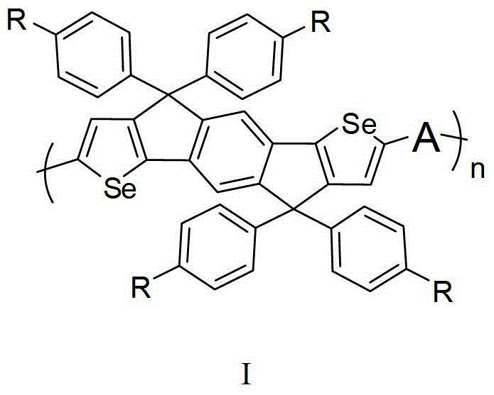
Diselenophenobenzodiindene conjugated polymer semiconductor materials and their applications
A technology of conjugated polymers and benzobisindene derivatives, which can be used in semiconductor devices, semiconductor/solid-state device manufacturing, electric solid-state devices, etc., can solve problems such as limited mobility, and achieve improved photovoltaic performance and high hole mobility. , the effect of improving the mobility
- Summary
- Abstract
- Description
- Claims
- Application Information
AI Technical Summary
Problems solved by technology
Method used
Image

Examples
Embodiment 1
[0024] When R is a 2-ethylhexyl chain, the monomer M can be expressed as the monomer M 1 , with the following structure:
[0025]
[0026] The monomer M of the embodiment of the present invention 1 The synthetic route of is as follows:
[0027]
[0028] Compound 1
[0029] Add 16.2g of 2,5-dibromoterephthalic acid (50mmol) and 40ml of thionyl chloride (SOCl 2 ) was heated to reflux for 12h, and when the solution became clear, SOCl was removed by atmospheric distillation 2 , adding petroleum ether, cooling to precipitate a solid, and suction filtration to obtain 17.1 g of compound 1 with a yield of 95%. 1 H-NMR (400MHz, CDCl 3 , δppm): 8.21 (s, 2H).
[0030] Compound 2
[0031] Under ice bath, to 200ml CH containing 7.2g (20mmol) compound 1 2 Cl 2 Slowly add 6.8g of crushed AlCl to the solution 3 (51mmol) powder, to be AlCl 3 After dissolution, 25 ml of CH containing 15.6 g of 2-ethylhexylbenzene (82 mmol) was added 2 Cl 2 solution. Stir at room temperature an...
Embodiment 2
[0041] The structural formula and synthetic route of the conjugated polymer material P(SePSe-2,4-BT) of the embodiment of the present invention are as follows:
[0042]
[0043] N 2 Under the protection of , add 0.504g (0.35mmol) of monomer M in a 50ml single-necked bottle 1 And 0.103g (0.35mmol) monomer a and 20mg tetrakis (triphenylphosphine) palladium [abbreviated as Pd (PPh 3 ) 4 ], add 20ml of anhydrous toluene, after heating to reflux for 48h, the reaction mixture is poured into methanol (500mL) for coagulation, the precipitation is filtered to obtain the first product, and the first product is extracted with methanol, acetone, and n-hexane respectively with a Soxhlet extractor. After extracting for 24 hours, the soluble part was collected with chloroform and vacuum-dried to obtain 340 mg of polymer material P(SePSe-2,4-BT), with a yield of 78%. 1 H-NMR (400MHz, CDCl 3 , δppm): 8.2-7.9 (br, 2H), 7.9-7.6 (br, 2H), 7.6-7.4 (br, 2H), 7.4-7.2 (br, 8H), 7.1-6.9 (br, 8H...
Embodiment 3
[0046] The structural formula and synthetic route of the conjugated polymer material P(SePSe-2,4-DTDPP) of the embodiment of the present invention are as follows:
[0047]
[0048] N 2 Under protection, 0.432g (0.3mmol) of monomer M 1 and 0.272g (0.3mmol) of monomer b and 17mg of Pd (PPh 3 ) 4 Dissolve in 20ml of anhydrous toluene, heat and reflux for 48h, pour the reaction mixture into methanol (500mL) for coagulation and precipitation, the precipitate is filtered to obtain the primary product, and the primary product is extracted with methanol, acetone, and n-hexane with a Soxhlet extractor, respectively. After extracting for 24 hours, the soluble part was collected with chloroform and vacuum-dried to obtain 470 mg of polymer material P(SePSe-2,4-DTDPP), with a yield of 84%. 1 H-NMR (400MHz, CDCl 3 , δppm): 9.0-8.7 (br, 2H), 7.5-7.3 (br, 4H), 7.3-7.1 (br, 10H), 7.1-6.9 (br, 8H), 4.2-3.8 (br, 4H), 2.75 -2.25(br, 8H), 2.1-1.8(br, 2H), 1.7-1.5(br, 4H), 1.5-1.0(br, 80H),...
PUM
 Abstract
Description
Claims
Application Information