
In-Sb-Te ternary phase change nanotube and preparation method of array thereof

An in-sb-te, nanotube technology, applied in nanotechnology, nanotechnology, nanotechnology for information processing, etc., can solve problems such as rare synthesis, achieve high repeatability, low synthesis temperature, and uniform size Effect

Inactive Publication Date: 2014-01-22
TIANJIN UNIV
View PDF3 Cites 1 Cited by
  • Summary
  • Abstract
  • Description
  • Claims
  • Application Information

AI Technical Summary

Problems solved by technology

At present, the preparation and phase change storage behavior of In–Sb–Te films have been systematically studied, but the synthesis of In–Sb–Te series nanomaterials with special morphology is still rare.

Method used


Image

  • In-Sb-Te ternary phase change nanotube and preparation method of array thereof
  • In-Sb-Te ternary phase change nanotube and preparation method of array thereof
  • In-Sb-Te ternary phase change nanotube and preparation method of array thereof

Examples


Embodiment 1

[0028] A pulse cycle parameter is: first deposit at -1.6V for 50ms, then at -1.4V for 50ms, then choose to deposit at -1.3V for 50ms, and finally at -0.4V for 50ms, continue to deposit 30 according to the pulse cycle parameters Minutes, black-gray precipitation can be seen; take out the template with deposits, then dissolve the template with sodium hydroxide solution, and centrifuge repeatedly to completely remove the template. Get the target product.

[0029] The SEM picture of the prepared 200nm In-Sb-Te nanotube array is as follows figure 1 with 2 As shown, it can be seen that the output of the In-Sb-Te nanotube array is large, the length is uniform, up to several microns, and the diameter distribution of the In-Sb-Te nanotube array is very uniform. Example 2:

Embodiment 2

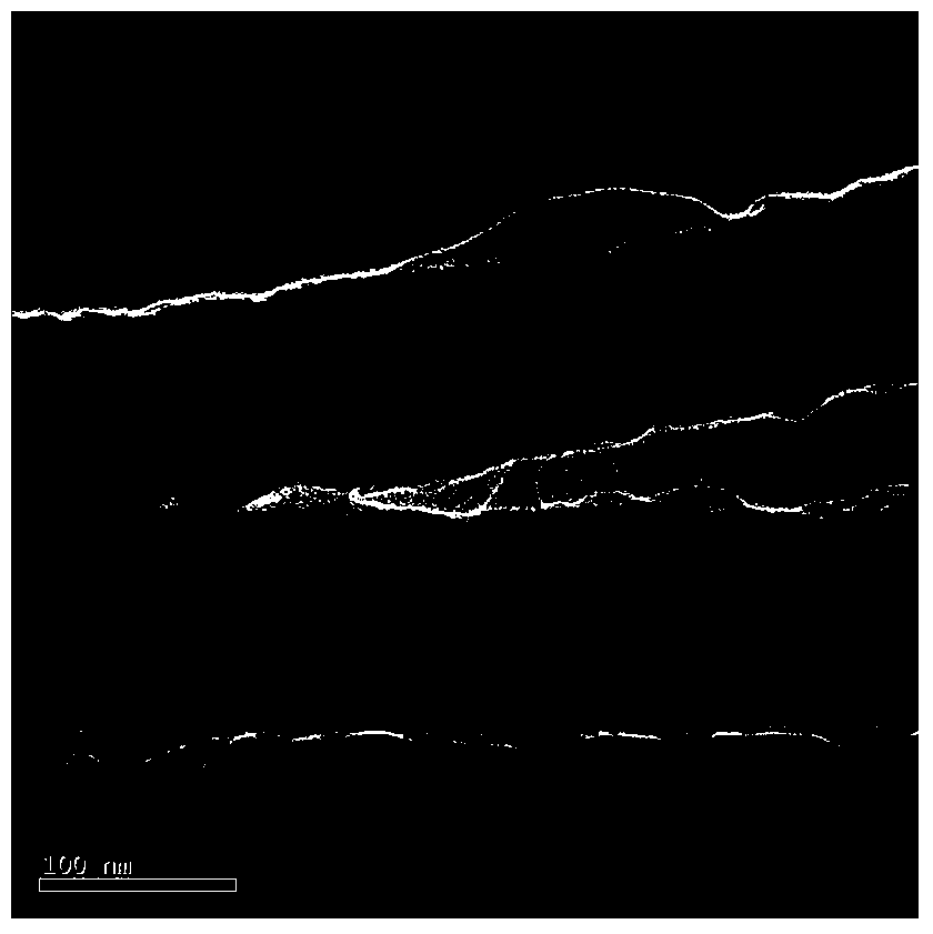
[0030] The steps are the same as in Example 1, except that the alumina template with a pore size of 200 nm is replaced with a polycarbonate (PC) template with a pore size of 100 nm, and other reaction conditions are kept unchanged, and the product is 100 nm In-Sb-Te nanotubes. TEM photos such as image 3 As shown, it is a nanotube structure with a tube wall of about 25nm.

Embodiment 3

[0032] The steps are the same as in Example 1, the difference is that the alumina template with a pore size of 200 nm is replaced with a polycarbonate (PC) template with a pore size of 400 nm, and the deposition time is extended to 1 hour. The other reaction conditions are kept unchanged.

[0033] In-Sb-Te nanotubes.

[0034] Perform energy spectrum eds analysis, the results are shown in the following table, the atomic content ratio of the three elements is 1.91:1.49:1, In 1.91 Sb 1.49 Te, the three elements in the prepared In-Sb-Te nanotubes are uniformly distributed along the axial direction at about 1:1:1, and indeed the tubular structure is distributed along the radial direction at 20-30nm. The content of In, Sb and Te Both decrease and rise again at 70-80nm, and the tube wall is about 25nm.

[0035] Element

[0036] From the reference "SynthesisandCharacterizationofGe2Sb2Te5NanowireswithMemory SwitchingEffect" YeonwoongJung,Se-HoLee,Dong-KyunKo,andRiteshAgarwal*J.AM.CHEM.SOC....


PUM

PropertyMeasurementUnit
Resistanceaaaaaaaaaa

Abstract

The invention discloses an In-Sb-Te ternary phase change nanotube and a preparation method of an array of the In-Sb-Te ternary phase change nanotube. A solution, of which the pH value is equal to 2.2, is prepared and is mixed with antimony chloride, indium chloride and potassium tellurite; one surface of a template is conductive, which is used as a working electrode; a reference electrode and a counter electrode are arranged in an electrolytic tank; electrolyte is transferred into the electrolytic tank; then the electrolytic tank is sealed and inert gas is introduced into the electrolytic tank to remove dissolved oxygen in the electrolyte; differential pulse electrodeposition is carried out. According to the In-Sb-Te nanotube, because a method of combining differential pulse electrodeposition process and a template process is adopted, the In-Sb-Te nanotube has the advantages of high yield, simple process, low synthetic temperature, uniform size, high repeatability and the like. The In-Sb-Te nanotube obtained by using the method has the nanoscale diameter, the length is from a few micrometers to dozens of micrometers, the size is uniform, and the nanotube is smooth and has an array structure; therefore, the nanotube is a good material with phase change property.

Description

Technical field [0001] The invention relates to a preparation method of a tellurium-based phase change storage nanometer material, and more specifically, to a one-dimensional In-Sb-Te ternary phase change nanotube and a preparation method thereof. Background technique [0002] Phase change random access memory (PCRAM, OUM) has the advantages of non-volatility, fast read and write speed, high storage density, low energy consumption, etc., as a replacement and development of the existing FLASH technology, attracting more and more researchers Explore new materials that can be used in phase change random access memory. Major semiconductor manufacturers (such as Intel, Ovonyx, Pillips, Samsung, Hitachi, etc.) continue to invest huge amounts of money to develop next-generation non-volatile, high-capacity memory chips. In July 2001, Intel released a 0.18μm 4MBOUM test chip. In 2003, Samsung Electronics also reported that it had successfully developed a small-capacity OUM. In May 2009,...

Claims


Application Information

Patent Timeline
IPC IPC(8): C25B1/00B82Y40/00B82Y10/00
Inventor 张兵许蕊吴睿黄义史艳梅
Owner TIANJIN UNIV
Learn More