Single photon emitter and manufacturing method thereof based on high refractive index contrast grating structure

A technology with high refractive index contrast and grating structure, which is applied in the direction of phonon exciters, lasers, laser components, etc., to achieve the effect of enhancing outgoing light, reducing difficulty, and increasing the wavelength adjustment range

Active Publication Date: 2014-01-22
INST OF SEMICONDUCTORS - CHINESE ACAD OF SCI
View PDF5 Cites 7 Cited by
  • Summary
  • Abstract
  • Description
  • Claims
  • Application Information

AI Technical Summary

Problems solved by technology

But usually this method by changing the distribution of light in the medium can only split the linear polarization into submillielectron volts

Method used


Image

  • Single photon emitter and manufacturing method thereof based on high refractive index contrast grating structure
  • Single photon emitter and manufacturing method thereof based on high refractive index contrast grating structure
  • Single photon emitter and manufacturing method thereof based on high refractive index contrast grating structure

Examples


Embodiment Construction

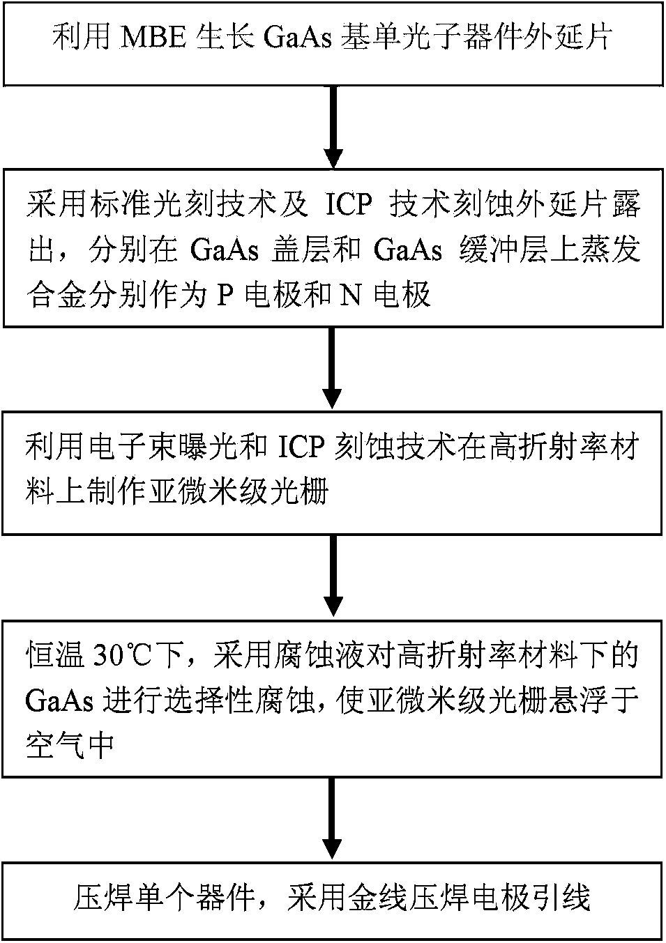
[0020] In order to make the object, technical solution and advantages of the present invention clearer, the present invention will be further described in detail below in conjunction with specific embodiments and with reference to the accompanying drawings.

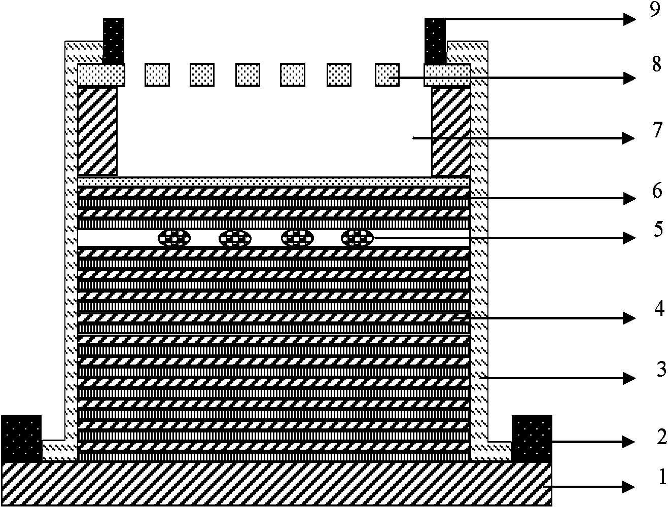
[0021] The single photon emitter based on the high refractive index contrast grating structure provided by the present invention first grows high-quality device epitaxial wafers on the GaAs substrate by molecular beam epitaxy technology, then uses surface emission technology to make electrodes, and finally uses electron beam Exposure produces a grating structure.

[0022] figure 1 It is a structural schematic diagram of a single photon emitter based on a high refractive index contrast grating structure provided by the present invention. Such as figure 1 As shown, the single photon emitter includes: GaAs buffer layer 1, N-type electrode 2, silicon dioxide passivation layer 3, lower DBR4, InAs quantum dot active region 5,...


PUM

PropertyMeasurementUnit
Thicknessaaaaaaaaaa

Abstract

The invention discloses a single photon emitter and a manufacturing method thereof based on a high refractive index contrast grating structure. The single photon emitter comprises a GaAs substrate, wherein an epitaxial wafer is prepared on the GaAs substrate, and comprises a GaAs buffer layer (1), DBR (Distributed Bragg Reflector) layers (4) and (6), an InAs quantum dot active area (5) and a high refractive index contrast grating (a low refractive index material (7) and a high refractive index material (8)) sequentially from the bottom up. The GaAs buffer layer is etched and exposed on the epitaxial wafer by adopting a standard photetching technology and an ICP (Inductively Coupled Plasma) technology to serve as an N-type ohmic contact layer, and then alloys are evaporated on the high refractive index material and the GaAs buffer layer respectively to serve as a P-type electrode and an N-type electrode. The submicron grating is manufactured on the high refractive index material by utilizing electron beam exposure and the ICP etching technology; a material of the lower layer of the grating is selectively corroded by utilizing a corrosive liquid; and a low refractive index air layer is obtained.

Description

technical field [0001] The invention relates to the technical fields of semiconductor technology, quantum computing and quantum information processing, in particular to a single photon emitter based on a high refractive index contrast grating structure and a manufacturing method thereof. Background technique [0002] With the huge expansion of society's demand for information, people's acquisition and processing of information has developed from one-dimensional space-time to two-dimensional. In addition to the mass transmission of information, the military pays more attention to the absolute security of information, and quantum information processing has also become an international frontier topic. It requires a large capacity for information transmission and requires absolute security of information, which is a huge challenge for information light sources. Single photon source is the key device to realize single photon qubit, optical quantum cryptography (quantum cryptogra...

Claims


Application Information

Patent Timeline
IPC IPC(8): H01S5/125H01S5/343
Inventor 王莉娟喻颖査国伟徐建星倪海桥牛智川
Owner INST OF SEMICONDUCTORS - CHINESE ACAD OF SCI
Why Eureka
Try Eureka