Online real-time representation device for film epitaxial growth

A technology of epitaxial growth and characterization, applied in Raman scattering, material excitation analysis, etc., which can solve problems such as uncertainty, error, and limited application

Active Publication Date: 2014-02-19
UNIV OF ELECTRONIC SCI & TECH OF CHINA
View PDF4 Cites 19 Cited by
  • Summary
  • Abstract
  • Description
  • Claims
  • Application Information

AI Technical Summary

Problems solved by technology

[0005] However, due to the particularity of MOCVD technology, the application of various characterization techniques in online monitoring is greatly limited.
[0006] 1. The reaction environment is full of various components and various concentrations of reaction gases, which greatly limits the characterization techniques that work by emitting electrons, such as reflection high-energy electron diffraction (RHEED), scanning electron microscopy (SEM), etc.
[0007] 2. The limited space of the reaction chamber and the rapidly rotating substrate limit the X-ray diffraction (XRD) technology that works in the scanning mode of variable grazing angle or variable wavelength.
However, due to the information obtained indirectly, there must be large errors

Method used


Image

  • Online real-time representation device for film epitaxial growth
  • Online real-time representation device for film epitaxial growth
  • Online real-time representation device for film epitaxial growth

Examples


Embodiment 1

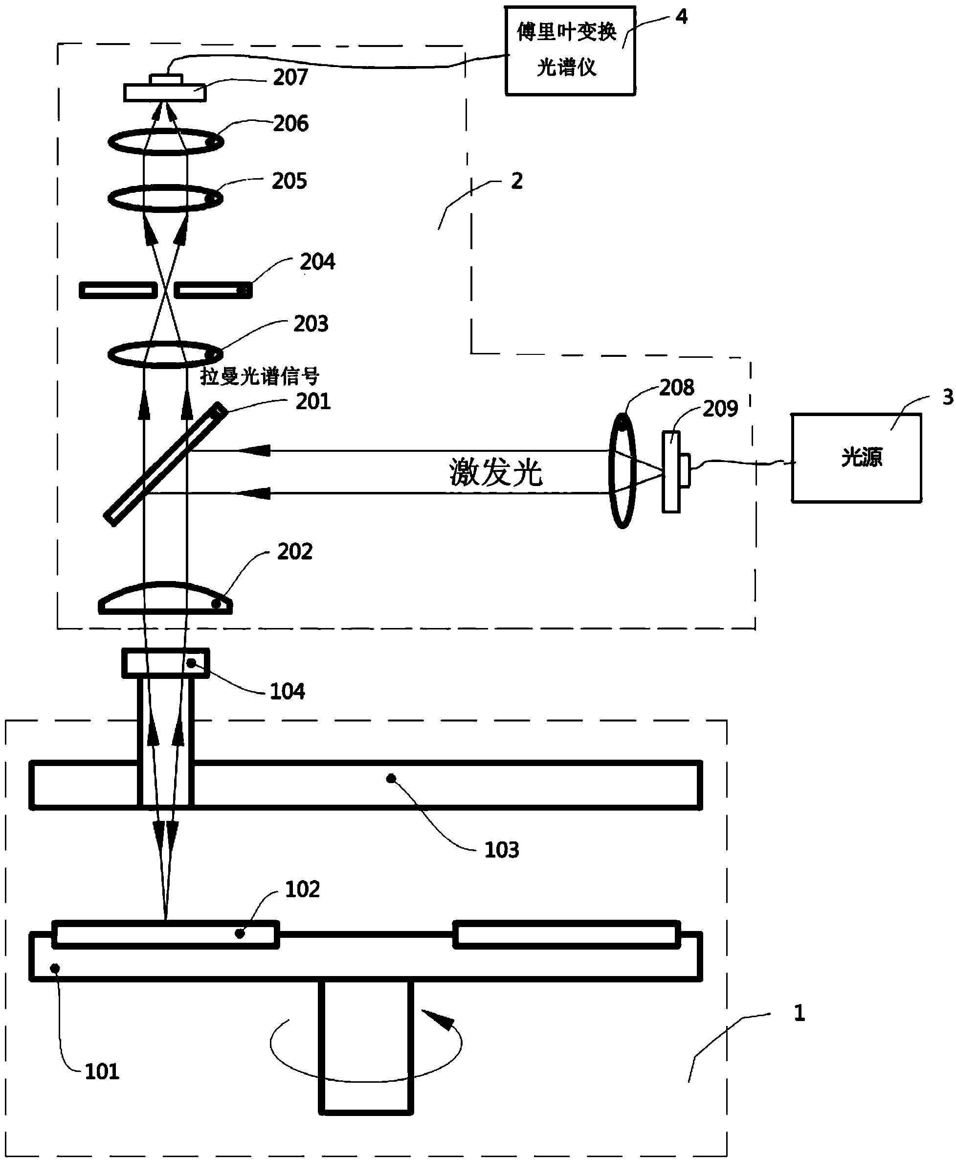
[0039] In this embodiment, as image 3 As shown, in order to achieve the above purpose of the invention, the online real-time characterization device for thin film epitaxial growth of the present invention includes a probe 2, a light source 3 and a Michelson interferometer 4;

[0040] The probe 2 includes a first beam splitter 201, a plano-convex lens 202, a first focusing lens 203, a confocal pinhole 204, a first collimating lens 205 and a second focusing lens 206; the light source 3 emits monochromatic excitation light After entering the probe 2 through the fiber coupler 209, it is transformed into parallel light by the straight lens 208, and after being reflected by the first beam splitter 201, it is focused by the plano-convex lens 202, and the focusing point is irradiated on the observation window 104 at the top of the MOCVD reaction chamber 1. On the epitaxial wafer 102 ; the Raman spectrum signal excited by the irradiated area of ​​the epitaxial wafer focusing point is co...

Embodiment 2

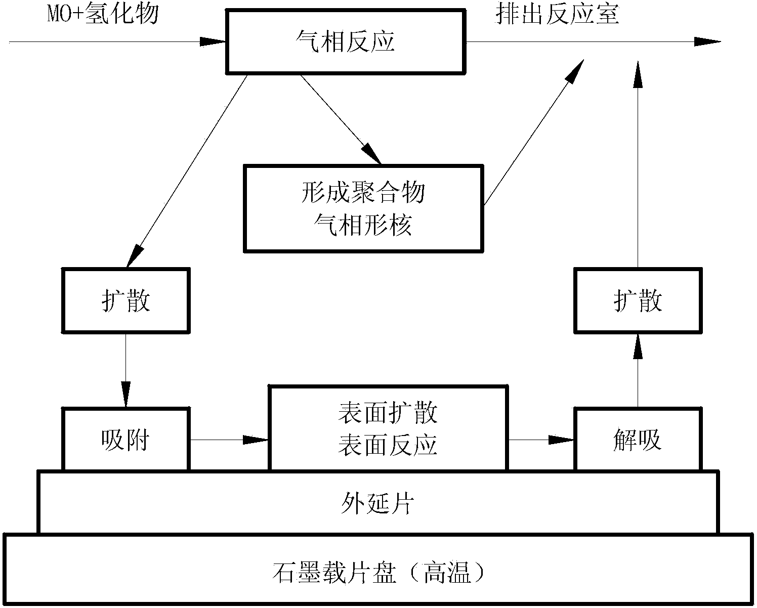
[0044] In this embodiment, on the basis of Embodiment 1, further improvements are made to enable online acquisition of reflection spectra and thermal radiation spectra. The reflected beam contains a large number of epitaxial wafer growth signals: reflecting the quality of surface atomic reconstruction , The reflection spectrum of the thickness of the epitaxial layer, and the thermal radiation spectrum of the temperature of the epitaxial wafer.

[0045] The Raman spectrum signal generated by the epitaxial wafer and the reflected beam including the reflection spectrum and the thermal radiation spectrum are divided into two beams by the first beam splitter 201 after passing through the plano-convex lens 202, one beam is transmitted for Raman spectrum detection, and the other beam is used for Raman spectrum detection. After reflection, it propagates in the opposite direction of the excitation light, such as Figure 4 shown. In the present invention, a second beam splitter 210 is ...

Embodiment 3

[0048] 1. Use the reflected spectral signal to accurately and repeat the positioning for the measurement of the Raman spectrum

[0049] Although the reflectivity of the epitaxial wafer 102 varies with the growth thickness, the reflectivity of the epitaxial wafer 102 is much higher than that of the graphite wafer plate 101 compared to the graphite wafer plate, so the measured reflection spectrum signal is the same as the graphite plate. The rotation of the slide disc 101 fluctuates, such as Figure 5 shown.

[0050] In the MOCVD process, in order to make the growth quality of the epitaxial wafer 102 as uniform as possible, the MOCVD equipment controls the rotation speed of the graphite carrier disk 101 very smoothly. Therefore, in this embodiment, on the basis of Embodiment 2, further improvements are made. The reflection spectrum signal detected by the detector 5 is analyzed in real time to obtain the relationship between the reflection spectrum fluctuation and the angular di...


PUM


Abstract

The invention discloses an online real-time representation device for film epitaxial growth. The online real-time representation device utilizes Raman spectroscopy signals to directly represent the microstructure of a nano material in MOCVD (Metal Organic Chemical Vapour Deposition) equipment in real time during a film epitaxial growth process. After reflected by a first spectroscope, excitation light is focused by a plane-convex lens, and the focus is radiated to an epitaxial wafer through an observing window in the top of the reaction cavity of the MOCVD equipment; since the Raman spectroscopy signals are excited in the radiation area of the focus of the plane-convex lens, most Raman spectroscopy signals are collected by the plane-convex lens; after passing through the first spectroscope, the Raman spectroscopy signals gather in the focus of the plane-convex lens, at the moment, a confocal pinhole is formed in the focus, and performs the function of space filtering and stray light resisting. The excitation light and the detection light (namely the Raman spectroscopy signals) share a light path front end unit, the size of a probe can be reduced as far as possible, and space limitation of the observing window of the reaction chamber is broken.

Description

technical field [0001] The invention belongs to the technical field of on-line monitoring, and more particularly relates to an on-line real-time characterization device for thin film epitaxial growth in MOCVD equipment. Background technique [0002] Metal Organic Chemical Vapour Deposition (MOCVD, Metal Organic Chemical Vapour Deposition) method is more and more widely used in the growth of nanomaterials due to its mature technology and good epitaxial growth quality, especially in the heteroepitaxial growth of GaN-based LEDs. Tool of. [0003] MOCVD is the use of metal organic compounds (MO) and hydrides, through chemical reactions such as cracking and synthesis in a high temperature reaction chamber, to perform thin film epitaxy growth on epitaxial wafers in the form of gas phase. [0004] As the structure of MOCVD epitaxial material growth becomes more and more complex, the components, atomic layer thickness and film quality that need to be controlled in the growth are ge...

Claims


Application Information

Patent Timeline
IPC IPC(8): G01N21/65
Inventor 王超陈磊伍思昕张晨贵梁莹林
Owner UNIV OF ELECTRONIC SCI & TECH OF CHINA
Why Eureka
Try Eureka