Method for manufacturing all-polymer plane optical path

A manufacturing method and a technology for a planar optical circuit, which are applied in the field of manufacturing an all-polymer planar optical circuit, can solve the problems of unfavorable high-performance optical waveguide device preparation, increase device scattering loss, and limit the scope of use, and achieve a large and strong replication cost advantage. Compatibility, simple process effect

Inactive Publication Date: 2014-02-19
SOUTH CHINA NORMAL UNIVERSITY
View PDF5 Cites 12 Cited by
  • Summary
  • Abstract
  • Description
  • Claims
  • Application Information

AI Technical Summary

Problems solved by technology

However, due to the large aspect ratio of MEMS and uTAS devices, choosing Si-LIGA and DEM technology and using Bosch process to etch the structure will inevitably cause circular jagged side walls, which will increase the reliability of optical waveguide devices. The scattering loss of large devices is not conducive to the preparation of high-performance optical waveguide devices, which undoubtedly limits its application range

Method used


Image

  • Method for manufacturing all-polymer plane optical path
  • Method for manufacturing all-polymer plane optical path
  • Method for manufacturing all-polymer plane optical path

Examples


Embodiment 1

[0052] Such as Figures 1 to 7 As shown, a method for fabricating an all-polymer planar optical path, wherein, Figure 7 It is a flow chart of this embodiment, and the specific steps are as follows:

[0053] Step (1), testing the optical properties of the polymer materials 31, 41, 51, using the waveguide theory of Maxwell's equations to conduct mode analysis and device propagation characteristic simulation. Obtain the device structure in the light wave single-mode or multi-mode transmission state. Then, according to the simulation parameters of the device, use computer-aided design tools to draw the mask layout of the device, mark the distribution of the planned device, and process and manufacture the mask plate for lithography.

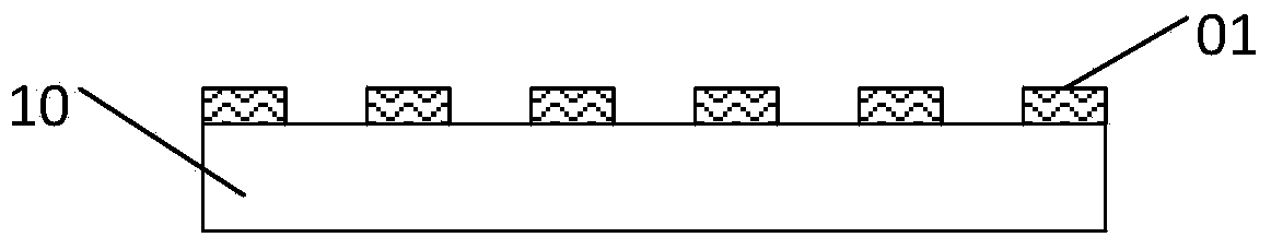
[0054] Step (2), spin-coat AZ5214 photoresist 01 on the conductive silicon wafer 10, use Suss MA6 equipped with a broadband light source for photolithography, first select the exposure mode, edit the exposure time, and then perform contact exposure...

Embodiment 2

[0062] The fabrication method of the all-polymer planar optical path of this embodiment still adopts Figure 1 to Figure 7 As an illustration, the specific steps are as follows:

[0063] Step (1), the test obtained cycloolefin material E48R (polymer material 31) has a refractive index of 1.518 at 1550nm, and the polysiloxane material OE-6550 (polymer material 41) has a refractive index of 1.532 at a wavelength of 1550nm . E48R is selected as the cover layer 51, and OE-6550 is used as the optical transmission medium. After simulation calculation, the structural size of single-mode transmission is W=H=5um, that is, when OE-6550 is used as the dielectric to transmit electromagnetic waves with a wavelength of 1550nm, the width and height of the core cross-sectional size of the single-mode transmission are both 5um.

[0064] Step (2), spin coating AZ5214 photoresist 01 on the silicon wafer 10, the spin coating speed is 4000rpm, the time is 30s, the pre-baking temperature is 95 de...

Embodiment 3

[0072] Step (1), test the refractive index of polymethacrylate PMMA (polymer material 31) at 1550nm is 1.479, the refractive index of polysiloxane material OE-6550 (polymer material 41) at 1550nm wavelength 1.532. PMMA is selected as the upper reflection layer 51, and OE-6550 is used as the light wave transmission medium. After simulation calculation, the structural size of single-mode transmission is W=H=3um.

[0073] Step (2), spin-coat AZ5214 photoresist 01 on the silicon wafer 10, the spin-coating speed is 4000rpm, the time is 30s, the pre-baking temperature is 95 degrees, the time is 90s, the exposure time is 6.8s, and after developing for 45s, no The cross-linked photoresist is removed in the developer, and finally the pattern structure of the mask is obtained on the photoresist 01.

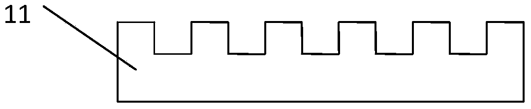
[0074] Step (3), harden the film at a temperature of 110 degrees for 90 seconds, put it into the deep silicon etching equipment of STS for dry etching, and then use acetone to ultrasonica...


PUM

PropertyMeasurementUnit
refractive indexaaaaaaaaaa

Abstract

The invention discloses a method for manufacturing an all-polymer plane optical path. The method comprises the steps of (1) obtaining an initial master mold by means of ultra-violet lithography and deep-etching technologies, duplicating a metallic nickel mold by means of electrochemical sedimentation, and manufacturing a polymer micro-structure part by means of mini molding; (2) conducting segment treatment on the part by means of the thermal annealing technology to reduce the roughness of the lateral wall and reduce scattering loss during optical wave transmission; (3) applying and filling polymer medium materials and obtaining the core structure of the plane optical path after the polymer medium materials are solidified; (4) combining a bondage layer of an element with an optical polymer substrate to achieve the manufacturing of the buried ridge type polymer plane optical path, wherein a polymer adhesive layer serves as the bondage layer of the element. Compared with a traditional method for manufacturing the polymer plane optical path, the method for manufacturing the all-polymer plane optical path has the advantages that cost is reduced and universality of technologies to materials is high.

Description

technical field [0001] The invention belongs to the technical field of optical element manufacturing, and in particular relates to a method for manufacturing an all-polymer plane optical path. Background technique [0002] Optical waveguides can be divided into inorganic optical waveguides and organic optical waveguides according to their dielectric materials. In the early stage, inorganic optical waveguides appeared, and their dielectric materials were inorganic substances, such as quartz glass. Compared with traditional inorganic optical waveguides, organic optical waveguides Organic materials, such as polymers, are used as the medium; the processing technology of organic optical waveguides is relatively simpler than that of inorganic optical waveguides. In terms of the manufacturing process of polymer optical waveguides, several main process methods have been born successively according to the manufacturing plan of the patterned waveguide core layer. [0003] Among these...

Claims


Application Information

Patent Timeline
Patent Type & Authority Applications(China)
IPC IPC(8): G02B6/13G02B6/136
Inventor 梅霆万磊李旋朱凝
Owner SOUTH CHINA NORMAL UNIVERSITY
Why Eureka
Try Eureka