

Gallium nitride homoepitaxy method based on in situ etching
A homoepitaxial and in-situ etching technology, applied in chemical instruments and methods, from chemically reactive gases, crystal growth, etc., can solve problems affecting the photoelectric properties of homoepitaxial materials, large residual stress, and high dislocation density , to achieve the effect of simple and easy method, improving crystal quality and reducing dislocation density
- Summary
- Abstract
- Description
- Claims
- Application Information
AI Technical Summary
Problems solved by technology
Method used
Image

Examples
Embodiment 1
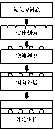
[0027] Embodiment 1: refer to figure 1
[0028] 1) Select a C-side self-supporting gallium nitride substrate, use acetone, ethanol and deionized water to sonicate for 5 minutes, and finally use high-purity nitrogen to blow off its moisture;
[0029] 2) Transfer the cleaned gallium nitride substrate to a metal organic chemical vapor deposition (MOCVD) system, with the front side (0001) facing up, the reaction chamber pressure is 100torr, heated to 1100°C, and 3000 sccmNH is introduced during the heating process 3 to protect
[0030] 3) Keep the pressure of the reaction chamber at 100torr, the temperature at 1100°C, and turn off the NH 3 , into H 2 , make the reaction chamber in a pure hydrogen atmosphere, and etch rapidly for 1 minute;
[0031] 4) Keep the pressure and temperature constant, and feed NH 3 , so that the reaction chamber is in the mixed gas of hydrogen and ammonia (H 2 :NH 3 =40:1) atmosphere, slow etching for 30 minutes;
[0032] 5) Keep the pressure and ...
Embodiment 2
[0035] 1) Select a C-side self-supporting gallium nitride substrate, use acetone, ethanol and deionized water to sonicate for 5 minutes, and finally use high-purity nitrogen to blow off its moisture;
[0036] 2) Transfer the cleaned gallium nitride substrate to a metal organic chemical vapor deposition (MOCVD) system, with the front side (0001) facing up, the reaction chamber pressure is 200torr, heated to 1050°C, and 3000 sccm is introduced during the heating process NH 3 for protection;
[0037] 3) Keep the reaction chamber pressure at 200torr, temperature at 1050°C, turn off NH3 , into H 2 , so that the reaction chamber is in a pure hydrogen atmosphere, rapid etching for 90 seconds;
[0038] 4) Keep the pressure and temperature constant, and feed NH 3 , so that the reaction chamber is in the mixed gas of hydrogen and ammonia (H 2 :NH 3 =30:1) atmosphere, slow etching for 40 minutes;
[0039] 5) The temperature rises to 1080°C, the pressure drops to 75torr, and the rea...
PUM
 Abstract
Description
Claims
Application Information