Fabrication method of gan-based ridge laser diode
A laser diode and ridge technology, applied in the directions of lasers, laser parts, semiconductor lasers, etc., can solve the problems of difficult alignment of the electrode window of the ridge laser diode, difficult to control the opening conditions of the insulating layer, etc., so as to avoid the plate alignment process. , Save the investment of equipment and manpower, and improve the effect of comprehensive performance
- Summary
- Abstract
- Description
- Claims
- Application Information
AI Technical Summary
Problems solved by technology
Method used
Image
Examples
Embodiment 1
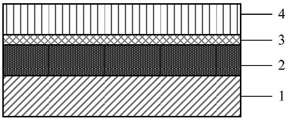
[0029] A GaN-based LD epitaxial layer 2 grown on a back-polished sapphire substrate 1, on the front of the GaN-based LD epitaxial layer 2, Ni / Au is deposited as a light-shielding layer 3 by electron beam deposition, and a photoresist is coated with a coater 4, such as Picture 1-1 shown.
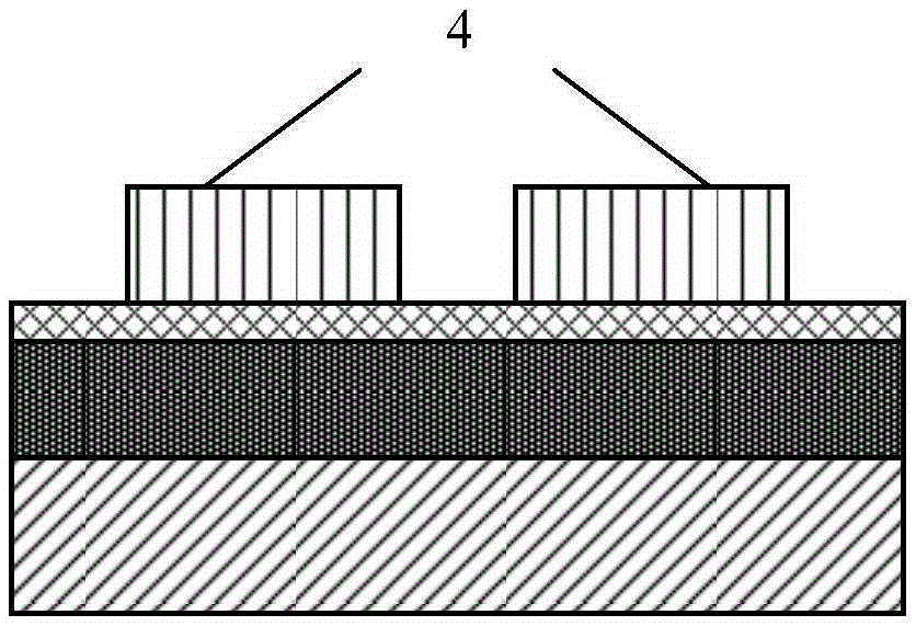
[0030] Use a ridge photolithography plate to expose, develop, and remove the base film with a plasma stripper to form a strip photoresist 4, such as Figure 1-2 shown.
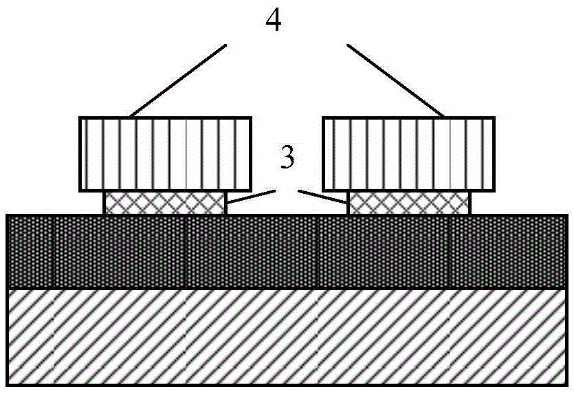
[0031] Use Ni / Au etching solution to etch the Ni / Au not protected by photoresist at room temperature, and the remaining Ni / Au light-shielding layer is strip-shaped 3, such as Figure 1-3 shown.
[0032] Use ICP to etch out the P-region ridge structure 5 of the laser diode, such as Figure 1-4 shown.
[0033] Clean the photoresist 4, and then anneal the alloy to form an ohmic contact, such as Figure 1-5 shown.
[0034] Coat photoresist 6 with a glue leveler, use an N-type mesa photolithography plate to pass through ex...
Embodiment 2
[0046] A GaN-based LD epitaxial layer 2 grown on a back-polished gallium nitride substrate, on the front side of the GaN-based LD epitaxial layer 2, Ni / Au is deposited as a light-shielding layer 3 by electron beam, and the photolithographic layer is coated with a coater Glue 4, such as diagram 2-1 shown.
[0047] Use a ridge photolithography plate to expose, develop, and remove the bottom film with a plasma stripper to form a strip photoresist, such as Figure 2-2 shown.
[0048] Use Ni / Au etching solution to etch the Ni / Au not protected by photoresist at room temperature, and the remaining Ni / Au light-shielding layer is strip-shaped 3, such as Figure 2-3 shown.
[0049] Use ICP to etch out the P-region ridge structure 5 of the laser diode, such as Figure 2-4 shown.
[0050] Clean the photoresist 4, and then anneal the alloy to form an ohmic contact, such as Figure 2-5 shown.
[0051] Apply a negative photosensitive heat-curing polyimide coating glue 10 on the epita...
PUM
 Abstract
Description
Claims
Application Information


