Manufacturing method of evanescent wave coupling high-speed high-power photoelectric detector

A technology of a photodetector and a manufacturing method, applied in the field of photodetectors, can solve problems such as large parasitic RC parameters, and achieve the effects of increasing doping concentration, reducing the difficulty of chip cleavage process, and reducing parasitic capacitance

Active Publication Date: 2014-03-19
THE 44TH INST OF CHINA ELECTRONICS TECH GROUP CORP
View PDF4 Cites 16 Cited by
  • Summary
  • Abstract
  • Description
  • Claims
  • Application Information

AI Technical Summary

Problems solved by technology

[0004] The technical problem to be solved by the embodiments of the present invention is to overcome the problem of large parasitic RC parameters introduced by the existing evanescent coupling optical waveguide and photodetector monolithic integrated chip manufacturing technology, and to provide an evanescent coupling type high-speed, high-power photoelectric How the detector is made

Method used


Image

  • Manufacturing method of evanescent wave coupling high-speed high-power photoelectric detector
  • Manufacturing method of evanescent wave coupling high-speed high-power photoelectric detector
  • Manufacturing method of evanescent wave coupling high-speed high-power photoelectric detector

Examples


Embodiment approach

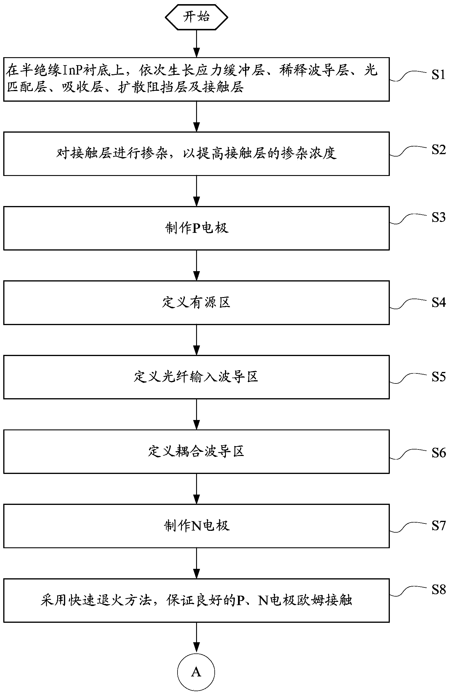
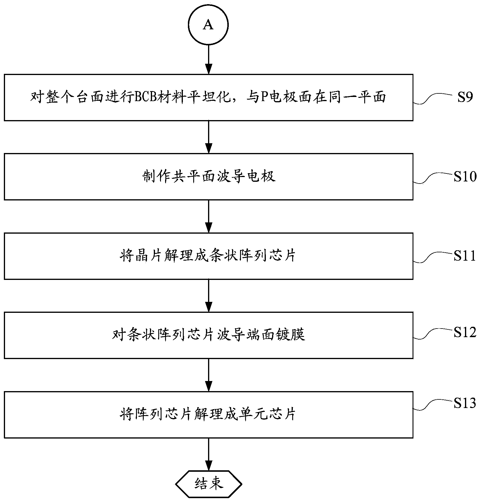
[0038] See Figure 1A and Figure 1B A preferred embodiment of the manufacturing method of the evanescent wave coupling type high-speed high-power photodetector of the present invention includes the following steps:

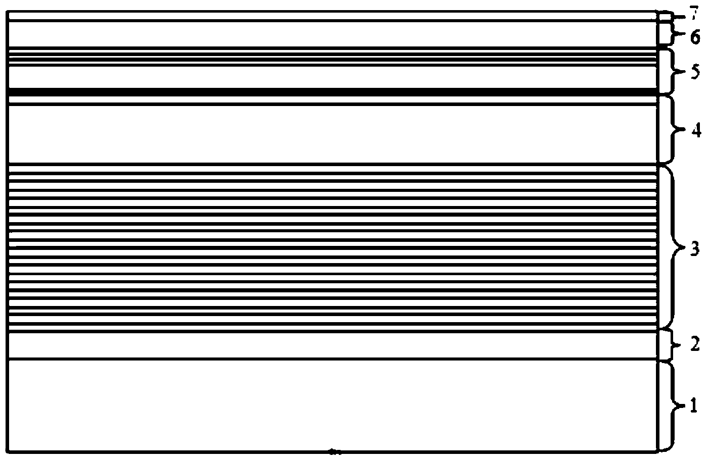
[0039] Step S1: On a semi-insulating InP substrate, a 100nm InP stress buffer layer, 10 cycles of InP / InGaAsP diluted waveguide layers, two layers (Q1.1, Q1 .4) InGaAsP optical matching layer, InGaAs absorption layer (including n-type, i-type, p-type), InP diffusion barrier layer, InGaAs contact layer, of which the stress buffer layer, diluted waveguide layer, optical matching layer, and absorption layer are hereinafter referred to as The diffusion barrier layer and the contact layer are collectively referred to as the epitaxial layer, and the substrate and the epitaxial layer are collectively referred to as the epitaxial wafer.

[0040]For details, please refer to figure 2 , which is a schematic cross-sectional view of epitaxially growing materials on an Fe-d...


PUM


Abstract

The invention comprises a manufacturing method of an evanescent wave coupling high-speed high-power photoelectric detector. The method comprises a, sequentially growing an InP stress buffering layer, ten cycle-alternating InP/InGaAsP diluted waveguide layers, two InGaAsP light matching layers, three InGaAs absorbing layers, an InP diffusion barrier layer and an InGaAs contact layer; b, doping the InGaAs contact layer through a Zn3As2 source; c, fabricating a P electrode; d, defining an active area; e, defining an optical fiber input waveguide area; f, defining a coupling waveguide area; g, fabricating an N electrode; h, guaranteeing good ohmic contact between the P electrode and the N electrode through a rapid annealing method; i, planarizing the whole table board through benzocylobutene materials to the same plane with the P electrode; j, fabricating coplanar waveguide electrodes; k, thinning epitaxial wafers to 110 mu m and cleaving the epitaxial wafers to strip array chips; l, coating film on the waveguide end surfaces of the strip array chips; m, cleaving the array chips into unit chips.

Description

technical field [0001] The invention relates to a photoelectric detector, in particular to a manufacturing method of an evanescent wave coupling type high-speed and high-power photoelectric detector. Background technique [0002] Evanescent wave coupled high-speed high-power photodetectors are the core devices in large-capacity optical fiber communication digital systems and broadband large-dynamic analog photonic systems. They can be used in conjunction with optical amplifiers to improve the sensitivity of high-speed digital communication systems. , can even generate a high enough photocurrent to directly drive the decision circuit without an electrical amplifier, which can also minimize the noise figure of the externally modulated analog photonic link and increase the dynamic range. [0003] In order to reduce the space charge effect and reduce the thermal resistance, the partially depleted (Partially depleted absorber-PDA) detector structure has attracted much attention. ...

Claims


Application Information

Patent Timeline
Patent Type & Authority Applications(China)
IPC IPC(8): H01L31/18
CPCH01L31/105H01L31/1844Y02P70/50
Inventor 崔大健高新江黄晓峰樊鹏王立
Owner THE 44TH INST OF CHINA ELECTRONICS TECH GROUP CORP
Why Eureka
Try Eureka