

Method of employing ion implantation to prepare ultra low surface doping concentration low sheet resistance silicon solar cell
A silicon solar cell, surface doping technology, applied in the direction of circuits, photovoltaic power generation, electrical components, etc., can solve the problems of reducing the shading area of the front surface of the cell, low concentration of junction defects, etc., to achieve improved electrical performance, flexible process, good controllability
- Summary
- Abstract
- Description
- Claims
- Application Information
AI Technical Summary
Problems solved by technology
Method used
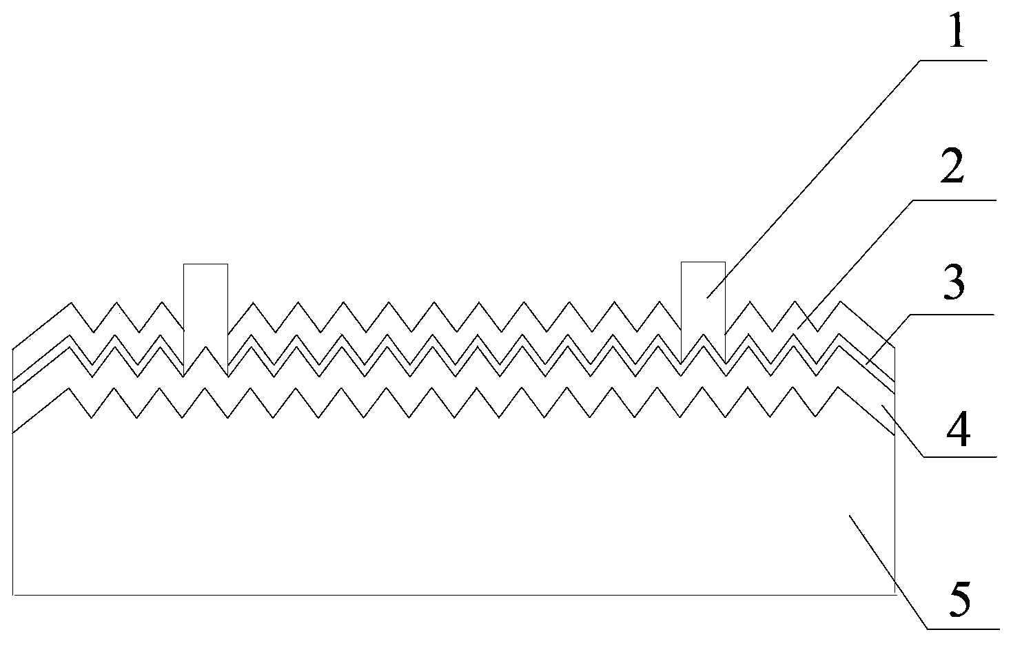
Image

Examples
Embodiment 1
[0034] A method for manufacturing a low square resistance silicon solar cell with an ultra-low surface doping concentration by ion implantation, comprising the following steps:
[0035] (1) Cleaning the surface of the P-type monocrystalline silicon wafer and making the textured surface is a surface formed by a pyramid, an inverted pyramid or a pit-like structure with a size of 0.1 to 100 microns;
[0036] (2) The method of ion implantation is used to inject phosphorus element into one side of the monocrystalline silicon wafer after texturing to form a PN junction, which specifically includes the following steps: fully cleaning the surface of the silicon wafer (including cleaning with ammonia water / hydrogen peroxide; cleaning with HCl / HF ), use an ion implanter to scan and implant P ions into the silicon wafer with an implantation energy of 30KeV, and then use a cleaning step (including ammonia / hydrogen peroxide, sulfuric acid / hydrogen peroxide, hydrochloric acid / hydrogen peroxi...
Embodiment 2
[0042] A method for manufacturing a low square resistance silicon solar cell with an ultra-low surface doping concentration by ion implantation, comprising the following steps:
[0043] (1) Cleaning the surface of the P-type monocrystalline silicon wafer and making the textured surface is a surface formed by a pyramid, an inverted pyramid or a pit-like structure with a size of 0.1 to 100 microns;
[0044](2) The method of ion implantation is used to inject phosphorus element into one side of the monocrystalline silicon wafer after texturing to form a PN junction, which specifically includes the following steps: fully cleaning the surface of the silicon wafer (including cleaning with ammonia water / hydrogen peroxide; cleaning with HCl / HF ), use an ion implanter to scan and implant P ions into the silicon wafer in 8 scans with an implantation energy of 5KeV, and then use a cleaning step (including ammonia / hydrogen peroxide, sulfuric acid / hydrogen peroxide, hydrochloric acid / hydrog...
Embodiment 3
[0050] Using the standard texturing method, the size of the pyramid on the suede surface is ~2um. After cleaning with HCl / HF, use an ion implanter to implant 2.8E15 doses of P with an implantation energy of 15KeV, and then wash with ammonia / hydrogen peroxide-HCl cleaning-HF cleaning After that, place the silicon wafer in 5-20% O 2 Anneal at 830-860°C for 10-20 minutes in a concentrated oxidizing atmosphere, (resistance after annealing is 80-85Ω / sq, ECV test shows that the surface concentration of phosphorus impurities is 3 , Junction depth is 0.3~0.5um), after annealing, use PECVD to plate SiNx film with a thickness of ~80nm, and finally use screen printing to complete metallization and sintering. After completion, the cell efficiency can reach 19.34% conversion efficiency.
PUM
| Property | Measurement | Unit |
|---|---|---|
| Size | aaaaa | aaaaa |
Abstract
Description
Claims
Application Information