A double-sided diffusion process for solar cells
A solar cell and double-sided diffusion technology, which is applied to circuits, photovoltaic power generation, electrical components, etc., can solve problems such as complex processes, easy denaturation, and complex components, so as to reduce the cost of process equipment, simplify the manufacturing process, and reduce manufacturing costs. Effect
- Summary
- Abstract
- Description
- Claims
- Application Information
AI Technical Summary
Problems solved by technology
Method used
Image
Examples
Embodiment 1
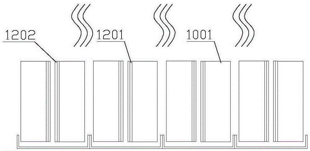
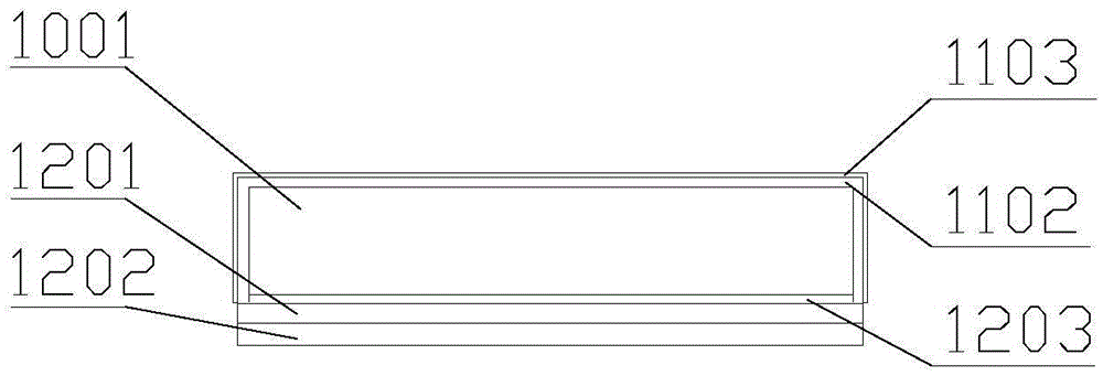
[0060] Such as Figures 1A-1G As shown, the double-sided diffusion process of the p-type crystalline silicon solar cell provided in this embodiment specifically includes the following steps: take the p-type crystalline silicon wafer 1001, remove the mechanical damage layer through chemical surface texturing, and remove the mechanical damage layer on the silicon wafer 1001. The surface of the sheet is cleaned with a 5% (wt) (mass percentage) dilute solution of hydrofluoric acid, and a nano-silica dispersion with a particle size of 90±50nm is used, and boron trioxide powder with a purity of 4N is added to Dilute with 18MΩ·cm deionized water, shake and mix evenly, spin-coat the dispersion on one side of the silicon wafer in a spin coater, which is the second surface of the so-called p-type silicon substrate, and dry at 200°C for 30min , solidify to form a coating 1201 containing impurity sources, and deposit a SiNx dielectric film 1202 with a thickness of 100 nm on the second sur...
Embodiment 2
[0062] Such as Figures 2A-2F As shown, the double-sided diffusion process of the p-type crystalline silicon wafer rear re-diffusion single-sided cell provided in this embodiment specifically includes the following steps: use the p-type crystalline silicon wafer 2001 to remove the mechanical damage layer at the same time through chemical surface texturing , the surface of the silicon wafer is cleaned with a 5% hydrofluoric acid dilute solution, a nano-silicon dioxide dispersion liquid with a particle size of 120±50nm is used, and boric acid with a purity of 99.8% is added, and deionized water of 18MΩ·cm Dilute and oscillate to mix evenly. Use ultrasonic atomization spraying to settle the mist droplets of the dispersion on one side of the silicon wafer, which is the second surface of the so-called p-type silicon substrate. Dry at 250°C for 20 minutes and solidify to form The coating 2201 containing the impurity source is deposited on the second surface with SiO with a thickness...
Embodiment 3
[0064] Such as Figures 3A-3F As shown, the double-sided diffusion process of the p-type crystalline silicon single-sided light-receiving cell provided in this embodiment specifically includes the following steps: the p-type crystalline silicon silicon wafer 3001 is chemically textured and the mechanical damage layer is removed at the same time. The surface of the silicon wafer is cleaned by a 5% dilute solution of hydrofluoric acid, a nano-silica dispersion with a particle size of 150±50nm is used, and boron trioxide powder with a purity of 4N is added, and 99.8% ethanol and deionized Dilute with water, shake and mix evenly, and deposit the dispersion liquid in the form of atomized droplets on the surface of one side of the silicon wafer, which is the second surface of the so-called p-type silicon substrate, by ultrasonic atomization spraying. The size of the template constrains the range of droplet deposition, so that the edge 3201' of the coating is finally smaller than the...
PUM
| Property | Measurement | Unit |
|---|---|---|
| particle diameter | aaaaa | aaaaa |
| electrical resistivity | aaaaa | aaaaa |
| thickness | aaaaa | aaaaa |
Abstract
Description
Claims
Application Information


