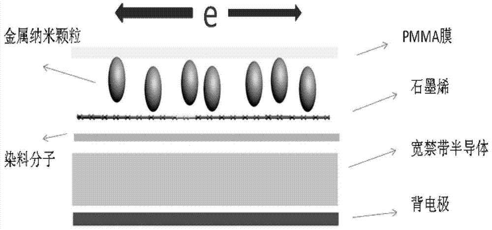
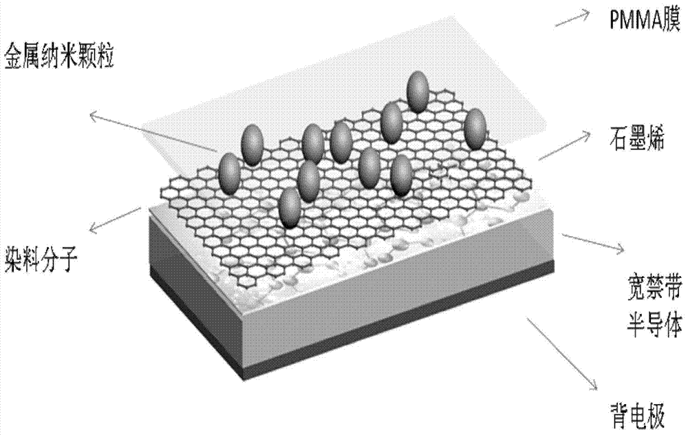
Solar cell based on surface plasma reinforcing principle and preparing method thereof
A surface plasmon and solar cell technology, applied in circuits, capacitors, photosensitive devices, etc., can solve problems such as poor thermal stability, and achieve the effects of increasing effective separation, facilitating flexible selection, and high safety performance.
- Summary
- Abstract
- Description
- Claims
- Application Information
AI Technical Summary
Problems solved by technology
Method used
Image
Examples
Embodiment 1
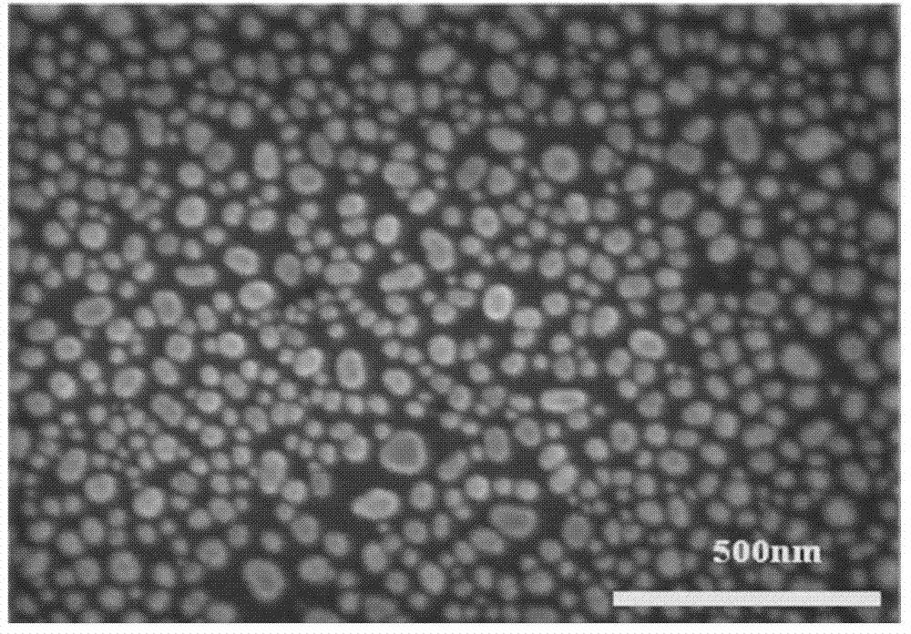
[0068] Embodiment 1. A solar cell device using single crystal zinc oxide as a wide bandgap semiconductor and K-19 dye as a photoexcitable dye; gold and silver are used as targets to vapor-deposit on graphene sheets.
[0069] The specific device preparation method is as follows:
[0070] 1. Preparation of ultra-flat zinc oxide wafers: prepare ultra-flat zinc oxide semiconductors (thickness 500nm) by magnetron sputtering, and then perform single-sided mechanical polishing on the zinc oxide wafers; Or ultrasonic cleaning in absolute ethanol for 30 minutes; then rinse with ultrapure water for 5 minutes, then rinse with deionized water for about 10 minutes, and finally blow dry with high-purity nitrogen.
[0071] 2. Evaporate low work function metals such as indium and silver on the non-mechanically polished side of the zinc oxide wafer as the back electrode; clamp the zinc oxide wafer to the top metal plate of the vacuum coating machine, so that the vacuum degree is pumped to 4.5×...
Embodiment 2
[0079] Embodiment 2, a solar cell device using monocrystalline titanium dioxide as a wide bandgap semiconductor and N719 dye as a photoexcitable dye; gold is evaporated on a graphene sheet as a target material.
[0080] The specific device preparation method is as follows:
[0081] 1. Preparation of ultra-flat titanium dioxide wafer: prepare ultra-flat titanium dioxide semiconductor (thickness is 300nm) by magnetron sputtering method, then perform single-sided mechanical polishing of titanium dioxide wafer; then etch with 35% HF aqueous solution for 8min, Then etch in 20W oxygen plasma for 80s.
[0082] 2. Evaporate low work function metals such as indium and silver on the non-mechanically polished side of the titanium dioxide wafer as the back electrode; clamp the titanium dioxide wafer on the top metal plate of the vacuum coating machine, so that the vacuum degree is pumped to 4.5×10 -4 Pa, according to the molar ratio of indium:silver of 1:1, it is vapor-deposited on the b...
Embodiment 3
[0089] Embodiment 3, a solar cell device using single crystal titanium dioxide as a wide bandgap semiconductor and Z907 dye as a photoexcitable dye; using pure silver as a target material to vapor-deposit on a graphene sheet.
[0090] The specific device preparation method is as follows:
[0091] 1. Preparation of ultra-flat titanium dioxide wafer: prepare ultra-flat titanium dioxide semiconductor (thickness 800nm) by magnetron sputtering method, and then perform single-sided mechanical polishing of titanium dioxide wafer; then etch with 35% HF aqueous solution for 8 minutes , and then etched in 20W oxygen plasma for 80s.
[0092] 2. Evaporate low work function metals such as indium and silver on the non-mechanically polished side of the titanium dioxide wafer as the back electrode; clamp the titanium dioxide wafer on the top metal plate of the vacuum coating machine, so that the vacuum degree is pumped to 4.5×10 -4 Pa, indium:silver is vapor-deposited on the back of the tita...
PUM
| Property | Measurement | Unit |
|---|---|---|
| Thickness | aaaaa | aaaaa |
| Thickness | aaaaa | aaaaa |
| Thickness | aaaaa | aaaaa |
Abstract
Description
Claims
Application Information


