Controllable preparation method of germanium-silicon nano lower-dimension structure and germanium-silicon nano lower-dimension structure

A dimensional structure and nano technology, which is applied in the field of controllable preparation of germanium and silicon nanometer low-dimensional structure, can solve the difficulty of semiconductor device processing technology, cannot precisely control position, size, morphology, and composition, and cannot realize nanometer low-dimensional structure. The structure is completely controllable preparation and other problems, to achieve the effect of high repeatability, good controllability and simple process steps

Inactive Publication Date: 2014-07-16
HUAZHONG UNIV OF SCI & TECH
View PDF5 Cites 10 Cited by
  • Summary
  • Abstract
  • Description
  • Claims
  • Application Information

AI Technical Summary

Problems solved by technology

[0005] In short, although the existing growth and preparation processes of silicon germanium nanowires and quantum dots are relatively mature, they cannot realize the fully controllable preparation of nanometer low-dimensional structures, and cannot precisely control each nanowire and each quantum dot. Key parameters such as point location, size, morphology, and composition have brought great technological difficulties to the processing of semiconductor devices based on germanium-silicon nano-structure at low temperature

Method used


Image

  • Controllable preparation method of germanium-silicon nano lower-dimension structure and germanium-silicon nano lower-dimension structure
  • Controllable preparation method of germanium-silicon nano lower-dimension structure and germanium-silicon nano lower-dimension structure
  • Controllable preparation method of germanium-silicon nano lower-dimension structure and germanium-silicon nano lower-dimension structure

Examples


Embodiment 1

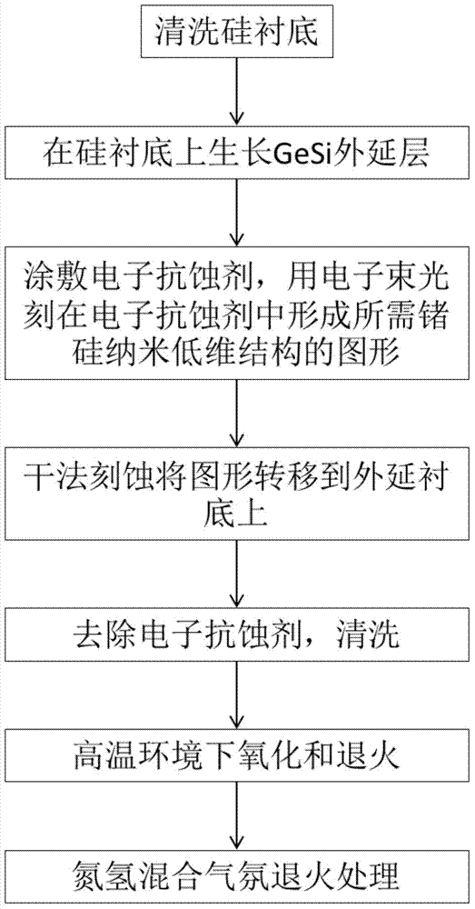
[0060] Periodically arranged silicon germanium nanowires with different sizes are prepared on the SOI substrate.

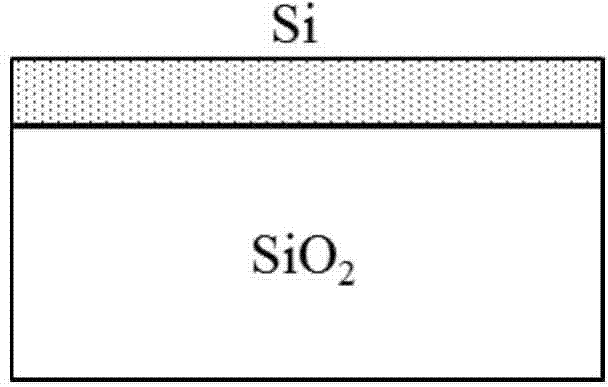
[0061] Such as diagram 2-1 As shown, the SOI substrate we selected (from bottom to top consists of a silicon base, a 3000nm thick buried oxide layer and a 55nm thick top layer silicon three-layer structure), and the substrate was cleaned by RCA process.

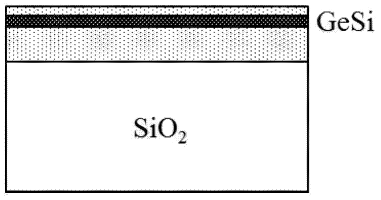
[0062] Figure 2-2 As shown, the SOI substrate is sent into the molecular beam epitaxy growth system, and 10nm silicon is grown at 450°C as a buffer layer, and then epitaxially grows Ge 0.1 Si 0.9 Quantum wells, 15nm thick, are finally covered with 5nm silicon. The molecular beam epitaxy system adopts the Eva-32 molecular beam epitaxy system of French Riber Company.

[0063] Figure 2-3 As shown, HSQ glue with a concentration of 3.6% is coated on the SOI substrate, the coating speed is 4000 rpm, and a hot plate is used for pre-baking at 150° C. for 4 minutes.

[0064] Figure 2-4 As shown, electron beam d...

Embodiment 2

[0070] Periodically arranged, germanium-silicon nanometer low-dimensional structures of different sizes are prepared on the SOI substrate.

[0071] Such as Pic 4-1 As shown, the SOI substrate we selected (from bottom to top is composed of a silicon base, a 3000nm thick buried oxide layer and a 53nm thick top layer silicon three-layer structure), and the substrate was cleaned by the RCA process.

[0072] Figure 4-2 As shown, the SOI substrate is sent into the molecular beam epitaxy growth system, and 10nm silicon is grown at 450°C as a buffer layer, and then epitaxially grows Ge 0.1 Si 0.9 Quantum wells, with a thickness of 30nm, are finally covered with 5nm silicon. The molecular beam epitaxy system adopts the Eva-32 molecular beam epitaxy system of French Riber Company.

[0073] Figure 4-3 As shown, the HSQ glue is coated on the SOI substrate, and pre-baked at 150°C for 4 minutes with a hot plate, and the thickness of the HSQ after baking is about 70nm.

[0074] Fi...

Embodiment 3

[0079] Periodically arranged, germanium-silicon nanometer low-dimensional structures of different sizes are prepared on the SOI substrate. According to the method provided by the invention, the concrete steps are:

[0080] Figure 6-1 As shown, the selected SOI substrate (from bottom to top consists of a silicon base, a 3000nm thick buried oxide layer and a 50nm thick top silicon three-layer structure), and the substrate is cleaned by RCA process.

[0081] Figure 6-2 As shown, the SOI substrate was sent into the ultra-high vacuum vapor deposition system, and 10nm silicon was grown as a buffer layer, and then epitaxially grown Ge 0.2 Si 0.8 Quantum wells, with a thickness of 30nm, are finally covered with 10nm silicon. Figure 6-3 As shown, ZEP520 glue is coated on the SOI substrate, the coating speed is 2000rpm, and a hot plate is used for pre-baking at 180°C for 3 minutes. After baking, the thickness of ZEP520 is about 90nm.

[0082] Figure 6-4 As shown, electron beam...


PUM

PropertyMeasurementUnit
thicknessaaaaaaaaaa

Abstract

The invention discloses a controllable preparation method of a germanium-silicon nano lower-dimension structure and the germanium-silicon nano lower-dimension structure. The controllable preparation method comprises the following steps of (a) cleaning a silicon substrate; (b) forming germanium-silicon alloy on the silicon substrate in an epitaxial growth mode to form an epitaxial substrate; (c) spreading electron resist and exposing the required germanium-silicon nano lower-dimension structure graph on the electron resist through the electron beam photolithography; (d) transferring the germanium-silicon nano lower-dimension structure graph to the epitaxial substrate through dry etching to obtain a sample; (e) removing the electron resist on the sample; (f) performing oxidation and anneal under a high-temperature environment to enable oxygen to react with silicon preferentially to form silicon oxide and germanium to be separated out; (g) performing anneal in a nitrogen and hydrogen mixing atmosphere to form the germanium-silicon nano lower-dimension structure. By means of the controllable preparation method, controllable preparation of the germanium-silicon nano lower-dimension structure in dimension, shape, position and component is achieved. Furthermore, the controllable preparation method has the advantages of being low in process difficulty, high in repeatability and capable of performing large-scale integration easily.

Description

technical field [0001] The invention belongs to the technical field of nano-processing of semiconductor devices, and in particular relates to a controllable preparation method and product of germanium-silicon nanometer low-dimensional structure. Background technique [0002] SiGe nano-low-dimensional structures are nanoscale structures with two-dimensional quantum confinement or three-dimensional quantum confinement, such as SiGe quantum dots and SiGe nanowires. They have gradually become a research hotspot in the field of integrated optoelectronics in recent years. The low-dimensional nanostructure of silicon germanium has the advantages of unique light emission and light absorption characteristics in the communication band, quantum confinement effect and Coulomb blockade effect, good carrier mobility, and compatibility with CMOS technology, etc., and has very broad application prospects. For example, silicon germanium quantum dots can be used to make on-chip integrated li...

Claims


Application Information

Patent Timeline
Patent Type & Authority Applications(China)
IPC IPC(8): H01L21/02H01L21/20B82Y40/00
CPCB82Y40/00H01L21/02532H01L21/02603H01L21/02664
Inventor 曾成夏金松张永
Owner HUAZHONG UNIV OF SCI & TECH
Why Eureka
Try Eureka