
Semi-conductor lead framework production process
A lead frame and production process technology, applied in the field of semiconductor lead frame manufacturing process, can solve the problems of large consumption, high production cost, poor coating adhesion, etc., to improve the slotting efficiency, reduce the slotting process, and reduce the width of copper tape precise effect
Patent Information
- Authority / Receiving Office
- CN · China
- Current Assignee / Owner
- Publication Date
- 2014-07-16
Smart Images
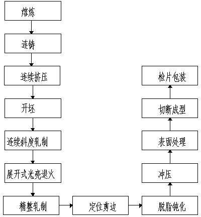
Figure 1 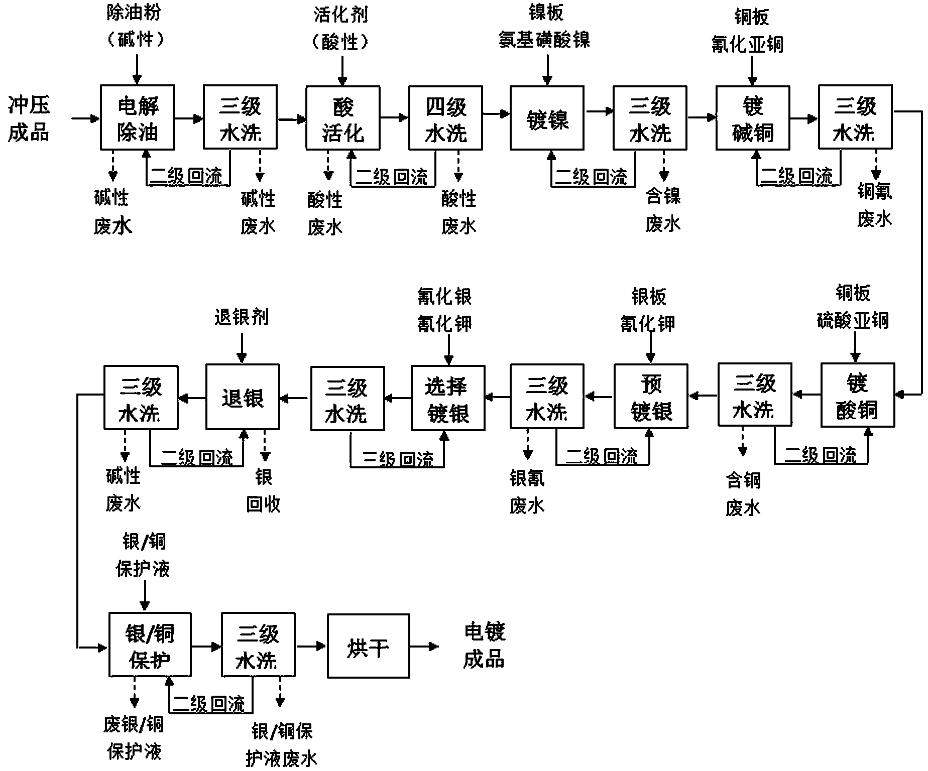
Figure 2 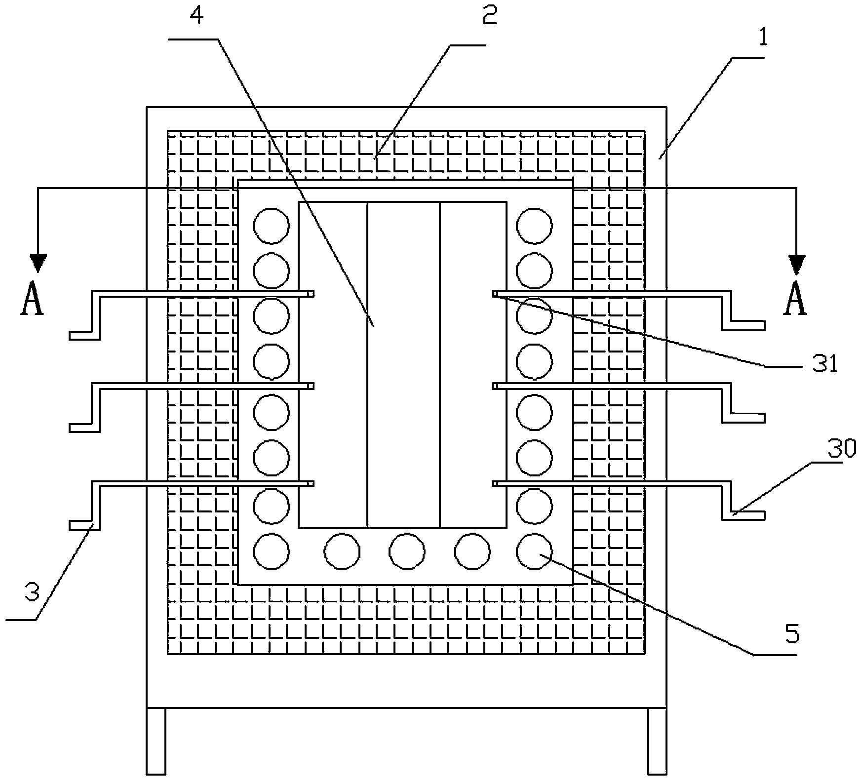
Figure 3
Abstract
Description
technical field
[0001] The invention relates to a manufacturing process for a semiconductor lead frame, in particular to a manufacturing process for manufacturing a semiconductor lead frame by using a mold stamping method. Background technique
[0002] Semi-conductive lead frame refers to a thin metal frame used to connect the contact point of the chip inside the semiconductor integrated block and the external wire. Its production raw material is mainly copper coil. Conventional semiconductor lead frames mainly have two manufacturing processes, one is etching method, and the other is die stamping method. The etching method is to etch a part of the material with a chemical substance to make a product, which is mostly suitable for small-scale production; the die stamping method is made by stamping the thin plate material conveyed intermittently by the stamping force of the mold, and is mostly suitable for large-scale production. The mold stamping method generally has the foll...
Examples
Embodiment 1
[0082] a. Melting: Copper is selected as the main raw material, and natural flake graphite is selected for oxygen barrier covering, and then smelted. During smelting, the temperature of the copper alloy is controlled within the range of 1080°C±10°C to obtain a copper alloy; in order to meet the requirements of high-power devices The performance of the copper is the selected composition of copper or the copper alloy grade of TFe 0.1 (KFC) copper. Further improve the electrical conductivity of the material. This process adopts a new type of specially selected copper alloy. The composition of the specially selected copper material is: Cu: ≥ 99.8%, P: 0.025-0.04%, Fe : 0. 05 ~ 0.15%, the balance is impurities.
[0083] b. Upward copper rod continuous casting: the copper alloy smelted in step a is cast into a copper alloy copper rod with a diameter of Φ16 mm and the same diameter by adopting the upward copper rod continuous casting method, and the copper alloy copper rod is wou...
Embodiment 2
[0098] In this implementation example: it is basically the same as in Example 1, the difference is that the specific structure of the annealing furnace used in the development type continuous bright annealing of this embodiment is: the annealing furnace includes an annealing furnace shell 1, and the annealing furnace shell 1 Both sides and the bottom of the inner wall are provided with a ceramic fiber layer 2, and the purpose of setting the ceramic fiber layer 2 is to keep heat and reduce heat loss in the annealing furnace. In order to prevent the copper coils from softening and extruding each other during annealing to cause curling and folding, we use a plurality of copper coil separators 3 to separate each independent copper coil to avoid mutual extrusion of each independent copper coil. The structure includes a partition 31 and a screw 30, and a threaded hole is provided on the annealing furnace shell 1 and the ceramic fiber layer 2, and the screw 30 passes through the annea...
Embodiment 3
[0108] This embodiment is basically the same as Embodiment 1, except that the specific structure of the cutting molding die used in the cutting molding process step is: comprising an upper mold, a lower mold, a cutting punch 17 and a forming punch 18, and the upper mold includes a fixed The backing plate 6 and the fixed plate 7, the fixed backing plate 6 is located above the fixed plate 7, the lower die includes a discharge backing plate 8 and a stripping plate 9, the unloading backing plate 8 is located above the stripping plate 9, and it is characterized in that: it also includes Upper slide block 12, lower slide block 13, left push block 11, right push block 10 and reset mechanism, the tail of the forming punch 18 is installed on the fixed plate 7, and the head of the forming punch 18 passes through the discharge backing plate 8 and the discharge plate 9, the forming punch 18 is provided with a longitudinal groove 16, the cutting punch 17 is arranged in the longitudinal groo...