Silicon carbide groove MOS junction barrier Schottky diode and manufacturing method thereof

A technology of junction barrier Schottky and silicon carbide trench, which is applied in the field of microelectronics, can solve the problems of reducing leakage current, low breakdown voltage, and serious concentration effect, so as to increase device reliability and reduce reverse leakage current Effect

Active Publication Date: 2014-07-16
XIDIAN UNIV
View PDF5 Cites 11 Cited by
  • Summary
  • Abstract
  • Description
  • Claims
  • Application Information

AI Technical Summary

Problems solved by technology

[0005] The purpose of the present invention is to overcome the above-mentioned shortcoming of the prior art, invent and design a kind of silicon carbide trench MOS junction barrier Schottky diode and its manufacturing method, mainly solve the problem that the device edge electric field concentration effect is serious and th

Method used


Image

  • Silicon carbide groove MOS junction barrier Schottky diode and manufacturing method thereof
  • Silicon carbide groove MOS junction barrier Schottky diode and manufacturing method thereof
  • Silicon carbide groove MOS junction barrier Schottky diode and manufacturing method thereof

Examples


Embodiment 1

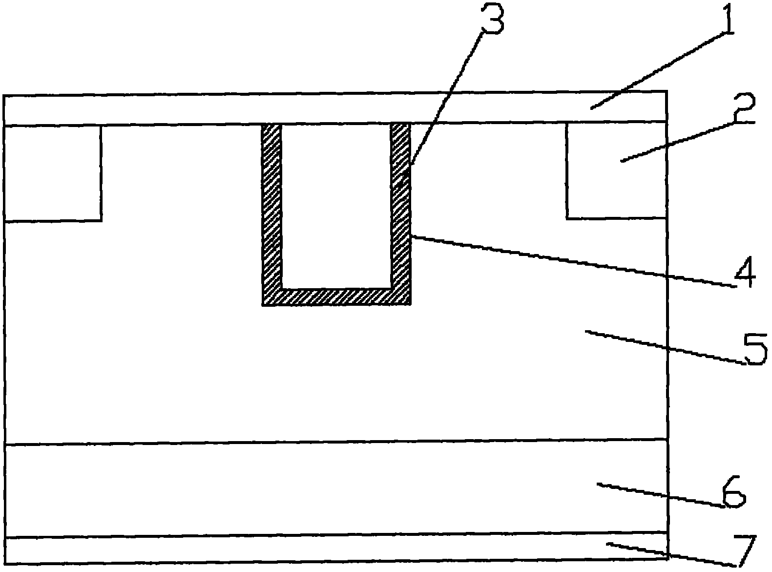
[0038] Step 1, in N + Epitaxial growth N on silicon carbide substrate - Drift layer, such as figure 2 .

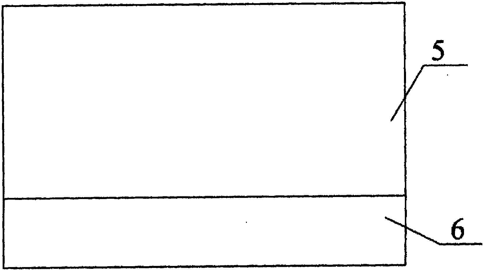
[0039] First on N + Type silicon carbide substrate 6 undergoes RCA standard cleaning; then on its front side, the epitaxial growth thickness is 10μm and the nitrogen ion doping concentration is 1×10 by low-pressure hot-wall chemical vapor deposition. 15 cm -3 Of N - In the epitaxial zone 5, the epitaxial process conditions are as follows: the temperature is 1580°C, the pressure is 100 mbar, the reaction gas is silane and propane, the carrier gas is pure hydrogen, and the impurity source is liquid nitrogen.

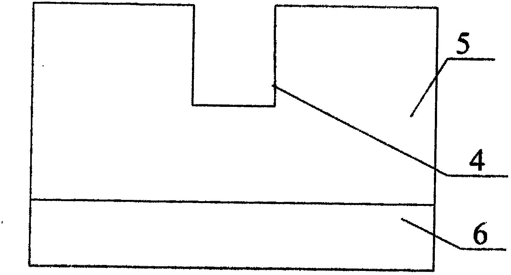
[0040] Step 2, in N - The epitaxial layer is etched to form trenches, such as image 3 .

[0041] In N - The epitaxial region 5 is first patterned by photolithography, and then 200nm of metal Ni is evaporated by ion beam evaporation, and an etching window is formed by stripping. The trench structure is formed by dry etching, where the etching gas is CF 4 +O 2 .

[0042] The t...


PUM

PropertyMeasurementUnit
Depthaaaaaaaaaa
Thicknessaaaaaaaaaa

Abstract

The invention discloses a silicon carbide groove MOS junction barrier Schottky diode and a manufacturing method of the silicon carbide groove MOS junction barrier Schottky diode. The problems of too low breakdown voltages, too low reliability and the like caused by the serious electric field concentration effect on the edge of a device and too high leakage currents are mainly solved. The silicon carbide groove MOS junction barrier Schottky diode and the manufacturing method are characterized in that a groove MOS structure is introduced on the basis of a traditional JBS device structure, and therefore the functions of relieving electric field concentration on a P-junction edge and lowering the leakage currents are achieved.

Description

Technical field [0001] The invention belongs to the technical field of microelectronics, and relates to a semiconductor device, particularly a silicon carbide trench MOS junction barrier Schottky diode and a preparation method thereof. Background technique [0002] Wide-gap semiconductor materials are third-generation semiconductor materials developed after the first-generation silicon, germanium, second-generation gallium arsenide, indium phosphide and other materials. Among the third-generation semiconductor materials, silicon carbide (SiC) and gallium nitride (GaN) are among the best. Silicon carbide material technology has matured, with high-quality 4-inch wafers. The gallium nitride material does not have a gallium nitride substrate, and the epitaxy can only rely on other materials. Its thermal conductivity is only one-fourth of that of silicon carbide, and it cannot achieve p-type doping. This restricts the application of gallium nitride materials in high-voltage and high...

Claims


Application Information

Patent Timeline
IPC IPC(8): H01L29/872H01L29/06H01L21/329H01L21/265
CPCH01L29/0615H01L29/6606H01L29/8725
Inventor 宋庆文袁昊汤晓燕张艺蒙贾仁需王悦湖张玉明
Owner XIDIAN UNIV
Why Eureka
Try Eureka