Method for preparing high-orientation small organic molecule semiconductor single-crystal patterns with controllable sizes

A technology of small molecules and semiconductors, which is applied in the field of preparing large-area, high-orientation and size-controllable organic small molecule semiconductor single crystal patterns, which can solve the problems of complex processing technology and difficulty in mass production, and achieve simplified processing technology, The effect of simple method

Inactive Publication Date: 2014-08-06
BEIHANG UNIV
View PDF4 Cites 14 Cited by
  • Summary
  • Abstract
  • Description
  • Claims
  • Application Information

AI Technical Summary

Problems solved by technology

The preparation of organic single crystal devices is mainly realized by manually selecting and positioning mobile single crystals. The processing technology is complicated and it is difficult to achieve mass production

Method used


Image

  • Method for preparing high-orientation small organic molecule semiconductor single-crystal patterns with controllable sizes
  • Method for preparing high-orientation small organic molecule semiconductor single-crystal patterns with controllable sizes
  • Method for preparing high-orientation small organic molecule semiconductor single-crystal patterns with controllable sizes

Examples


Embodiment 1

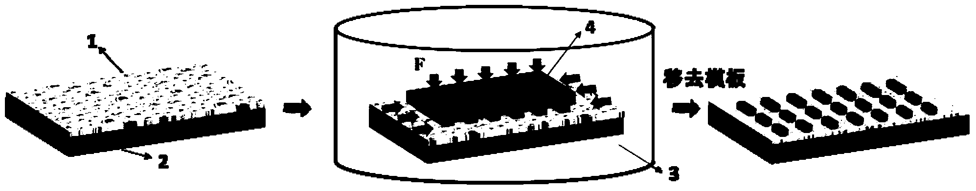
[0035] Example 1: The preparation of highly oriented anthracene stripe single crystal patterns with controllable large-area size, the steps are as follows:

[0036] The first step is to perform anti-sticking treatment on the silicon template. The silicon template was subjected to deionized water, acetone, ethanol, ultrasonic cleaning for 5 minutes, and oxygen plasma treatment for 2 minutes. Then place the silicon template in a desiccator filled with vapor of perfluorododecyltrichlorosilane (1H,1H,2H,2H-Perfluorodecyltrichlorosilane) and heat it at 90°C for 4h, and take it out for use. As the silicon template, 12 μm, 22 μm, 32 μm, and 52 μm stripe templates with equal intervals are selected.

[0037] In the second step, a 7% (mass percent) tetrahydrofuran mixed solution of anthracene / PMMA is configured, wherein the mass ratio of anthracene to PMMA is anthracene:PMMA=1:1, and the solution is left for 24 hours to fully dissolve. The silicon substrate was ultrasonically cleane...

Embodiment 2

[0040] Example 2: The preparation of high-orientation TIPS-PEN stripe single crystal pattern with large area and size controllable, the steps are as follows:

[0041] The first step is to perform anti-sticking treatment on the 5μm, 15μm, 22μm, 32μm, 52μm striped silicon templates with equal spacing. The silicon template was ultrasonically cleaned with deionized water, acetone and ethanol for 5 minutes, and treated with oxygen plasma for 2 minutes. Then place the silicon template in a desiccator filled with perfluorododecyltrichlorosilane (1H,1H,2H,2H-Perfluorodecyltrichlorosilane) and heat it at 90°C for 4h, and take it out for use.

[0042] In the second step, a 4% (mass percentage) mixed solution of TIPS-PEN / PS in chloroform was prepared (TIPS-PEN:PS=1:1, mass ratio), and left for 24 hours to fully dissolve the solution. The glass substrate was ultrasonically cleaned for 5 minutes as follows: ultrasonically cleaned with deionized water, acetone and ethanol, and finally tr...

Embodiment 3

[0045] Example 3: The preparation of high-orientation TIPS-PEN stripe single crystal pattern with large area and size controllable, the steps are as follows:

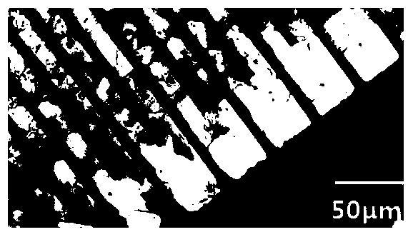
[0046] Prepare 1%, 2%, 3%, and 4% TIPS-PEN / PS mixed solutions respectively, and prepare mixed films by drop coating, and treat the samples in saturated toluene organic vapor at 60°C for 10 hours, and the remaining steps are the same as Example 2 is the same.

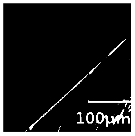
[0047] The test results show that TIPS-PEN single crystal patterns with a width of 5 μm, 15 μm, 22 μm, 32 μm and 52 μm can be prepared with large area and high orientation.


PUM


Abstract

The invention discloses a method for preparing high-orientation small organic molecule semiconductor single-crystal patterns with the controllable sizes. The method is based on capillary force etching and polymer auxiliary organic vapor treatment. In addition, solvent softening samples are utilized, so that the method is different from traditional capillary force etching. In a polymer auxiliary organic vapor treatment and capillary force etching process, a small organic molecule semiconductor / polymer compound membrane in tight contact with a mould plate is exposed in saturate organic vapor to be softened and even resolved partially. Under the capillary force action, polymer can drive a small organic molecule semiconductor to climb up along the lateral wall of the mould plate to be filled into a groove which is formed between the mould plate and a substrate. The small organic molecule semiconductor trends to be recrystallized under the dual action of the limit of patterns of the mould plate and the capillary force. Finally, a high-orientation small organic semiconductor single-crystal micro structure is formed on polymer. The organic vapor and the polymer can provide media for recrystallization of the small organic molecule semiconductor. The method can form large-size, even-size and high-orientation small organic molecule semiconductor patterns on the surface of the polymer by regulating the kind of polymer, the concentration of mixed solution, the kind of organic solvents and vapor pressure.

Description

technical field [0001] The invention relates to a method for preparing an organic small molecule semiconductor single crystal pattern. More specifically, the present invention provides a method for preparing large-area, high-orientation, and size-controllable organic small molecule semiconductor single crystal patterns. Background technique [0002] Organic / polymer semiconductor materials are attracting worldwide attention due to their outstanding photoelectric performance, low production cost, simple processing technology, wide range of material selection, convenient property adjustment, easy fabrication of large-area devices, and good combination with flexible substrates. inner gaze. Devices prepared using organic semiconductor materials as active layers, such as organic field effect transistors (organic [0003] field effect transistor (OFET), organic light-emitting diodes (organic light-emitting diodes, OLED), organic solar cells (organic solar cells) and organic solid...

Claims


Application Information

Patent Timeline
Patent Type & Authority Applications(China)
IPC IPC(8): H01L51/00H01L51/40
CPCH10K71/12H10K71/441
Inventor 王哲高明圆吴君辉袁艺
Owner BEIHANG UNIV
Why Eureka
Try Eureka