Organic light-emitting device and preparation method thereof

An electroluminescent device and luminescent technology, which is applied in the direction of electric solid-state devices, semiconductor/solid-state device manufacturing, electrical components, etc., can solve the problems of exciton quenching, general thermal stability, long diffusion distance, etc., and achieve high glass Transformation temperature, excellent electron transport performance, and good film-forming performance

Inactive Publication Date: 2014-09-17
OCEANS KING LIGHTING SCI&TECH CO LTD +2
View PDF6 Cites 4 Cited by
  • Summary
  • Abstract
  • Description
  • Claims
  • Application Information

AI Technical Summary

Problems solved by technology

However, there are also some problems, such as some P dopants, such as the general thermal stability of F4-TCNQ. During the use of the device, the doping structure itself is unstable, especially for the n-doped electron transport layer. Generally speaking, alkali metal compounds are usually used for doping, but the alkali metal ions are usually small in size, strong in diffusion ability, and have a long diffusion distance in the organic layer. In addition to being doped in the transport layer, alkali metal ions may also diffuse to In the light-emitting layer, it directly leads to the quenching of excitons, which affects the light efficiency and life of the device

Method used


Image

  • Organic light-emitting device and preparation method thereof
  • Organic light-emitting device and preparation method thereof
  • Organic light-emitting device and preparation method thereof

Examples


preparation example Construction

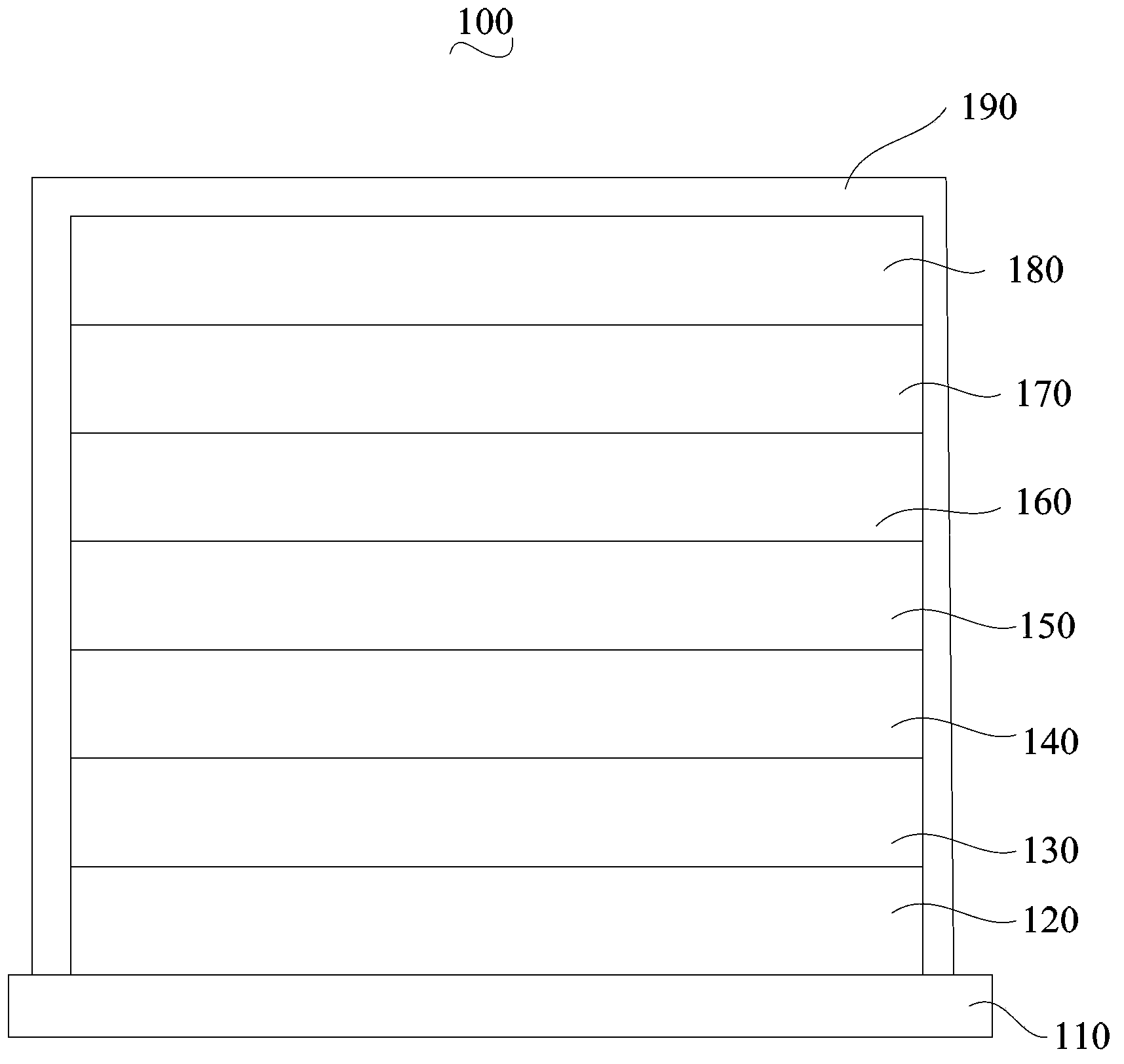
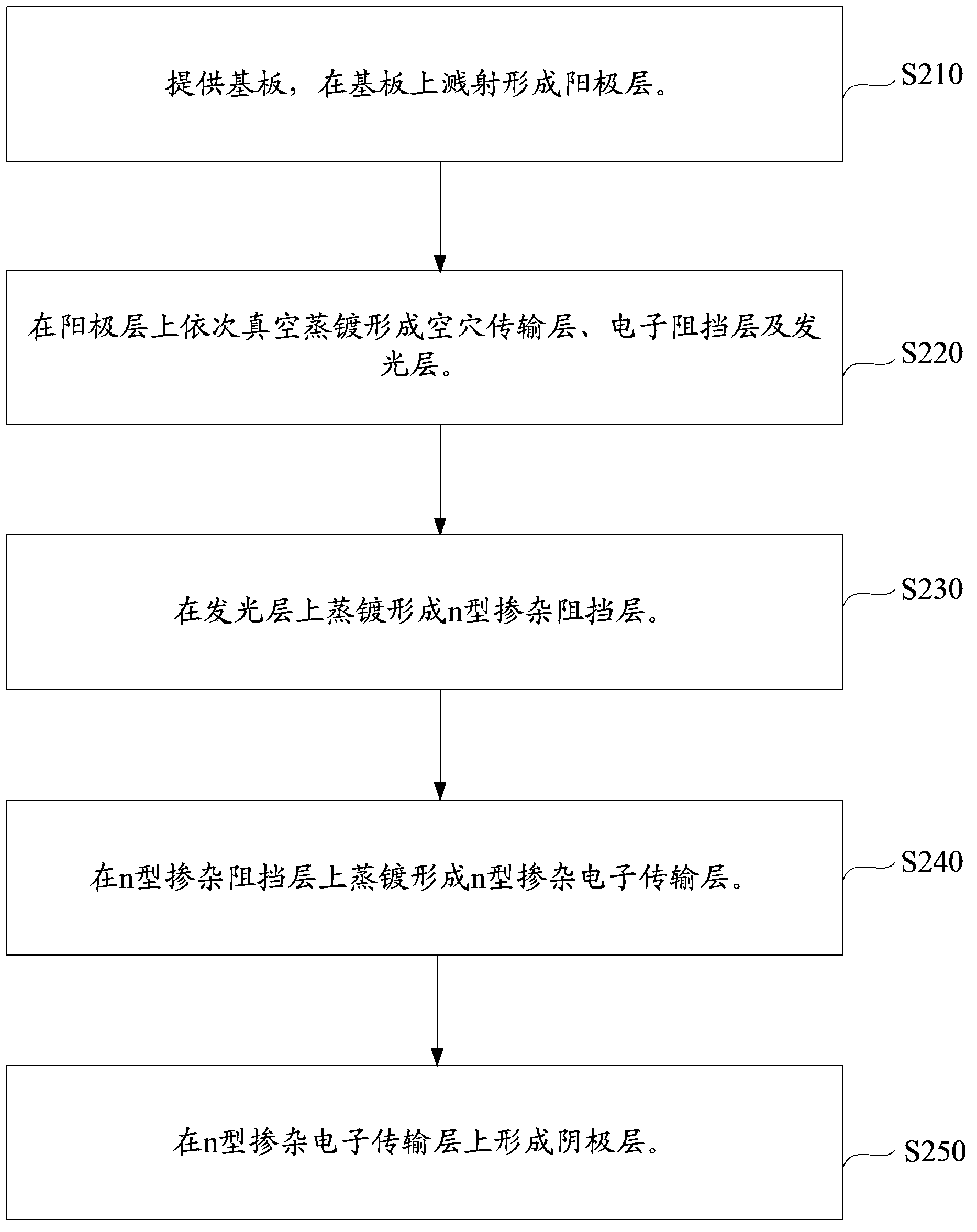
[0058] Such as figure 2 Shown, the preparation method of the organic electroluminescent device of one embodiment, comprises the following steps:

[0059] Step S210: providing a substrate, and forming an anode layer on the substrate by sputtering.

[0060] Preferably, the sputtering method is magnetron sputtering.

[0061] Preferably, before forming the anode layer by sputtering on the substrate, a cleaning step of the substrate is also included: the substrate is placed in deionized water containing detergent, isopropanol and acetone for ultrasonic cleaning, and then dried. In a specific embodiment, the substrate is placed in isopropanol and acetone and cleaned by ultrasonic waves for 20 minutes respectively; the cleaned substrate is dried by nitrogen gas.

[0062] Step S220: sequentially vacuum-evaporating a hole transport layer, an electron blocking layer, and a light emitting layer on the anode layer.

[0063] Preferably, the vacuum degree during vacuum evaporation is 10...

Embodiment 1

[0072] The structure of the organic electroluminescent device of the present embodiment is: glass / ITO / F6-TNAP:MeO-TPD / TAPC / Ir(ppy) 3 :TPBi / BAlq:Bphen / CsN 3 :Bphen / Ag.

[0073] The preparation of the organic electroluminescent device of this embodiment is as follows:

[0074] (1) Form the ITO anode layer by sputtering on the glass substrate: place the glass substrate in deionized water containing detergent for ultrasonic cleaning. blow dry. Then, an ITO anode layer is formed on the glass surface by magnetron sputtering, and the thickness of the anode layer is 100 nanometers. The glass substrate formed with the ITO anode layer is placed in a plasma treatment chamber for plasma treatment.

[0075] (2) Vacuum evaporation on the ITO anode layer to form a hole transport layer, an electron blocking layer and a light-emitting layer in sequence: the vacuum degree is 5×10 -4 Pa, where the material of the hole transport layer is 1,3,4,5,7,8-hexafluoro-tetracyano-dimethyl-p-naphthoqu...

Embodiment 2

[0081] The structure of the organic electroluminescent device of this embodiment is: glass / ITO / MoO 3 :2-TNATA / TAPC / Ir(MDQ) 2 (acac):NPB / Gaq 3 :Bphen / LiN 3 :TPBi / Al.

[0082] The preparation of the organic electroluminescent device of this embodiment is as follows:

[0083] (1) Form the ITO anode layer by sputtering on the glass substrate: place the glass substrate in deionized water containing detergent for ultrasonic cleaning. blow dry. Then, an ITO anode layer is formed on the glass surface by magnetron sputtering, and the thickness of the anode layer is 70 nanometers. The glass substrate formed with the ITO anode layer is placed in a plasma treatment chamber for plasma treatment.

[0084] (2) Vacuum evaporation on the ITO anode layer to form a hole transport layer, an electron blocking layer and a light-emitting layer in sequence: the vacuum degree is 1×10 -5 Pa, where the material of the hole transport layer is molybdenum oxide (MoO 3 ) doped 4,4',4''-tris(2-naphth...


PUM


Abstract

Disclosed is an organic light-emitting device which includes a substrate, an anode layer, a hole transmission layer, an electronic barrier layer, a light-emitting layer, an n-type doped barrier layer, an n-type doped electronic transmission layer and a cathode layer. The material of the n-type doped barrier layer is formed through mixing of an organic material and an organic metal compound, wherein the organic material is 4,7-diphenyl-o-phenanthroline or 2-(4-biphenylyl)-5-(4-tertiary butyl) phenyl-1,3,4-oxadiazole. The organic metal compound is formed through cooperation of one of beryllium, gallium, zinc, indium and aluminum and one of hydroxyquinoline, hydroxyquinoline derivative, hydroxyl benzoquinoline, and hydroxyl benzoquinoline derivative, wherein the organic material covers 30-70% of the material of the n-type doped barrier layer by mass. The organic light-emitting device is higher in light-emitting efficiency and longer in service life. Moreover, a preparation method for the organic light-emitting device is also provided.

Description

technical field [0001] The invention relates to the field of electronic devices, in particular to an organic electroluminescent device and a preparation method thereof. Background technique [0002] Organic electroluminescent diodes have a sandwich-like structure, with a cathode and an anode at the top and bottom, and a single or multiple functional layers of organic materials of different materials and structures sandwiched between the two electrodes, followed by hole injection. layer, hole transport layer, light emitting layer, electron transport layer and electron injection layer. The organic electroluminescent device is a carrier-injection light-emitting device. After the anode and the cathode are applied with an operating voltage, holes are injected from the anode and electrons from the cathode into the organic material layer of the working device respectively. Hole-electron pairs are formed in the luminescent material to emit light, and then the light is emitted from ...

Claims


Application Information

Patent Timeline
Patent Type & Authority Applications(China)
IPC IPC(8): H01L51/50H01L51/54H01L51/56
CPCH10K71/166H10K85/321H10K85/326H10K85/324H10K50/18H10K71/00
Inventor 周明杰王平冯小明钟铁涛
Owner OCEANS KING LIGHTING SCI&TECH CO LTD
Why Eureka
Try Eureka