

Organic light-emitting diode device and manufacturing method thereof
An electroluminescent device, organic technology, applied in the direction of electric solid-state devices, semiconductor/solid-state device manufacturing, electrical components, etc., can solve the problem of low lumen efficiency
- Summary
- Abstract
- Description
- Claims
- Application Information
AI Technical Summary
Problems solved by technology
Method used
Image

Examples
preparation example Construction
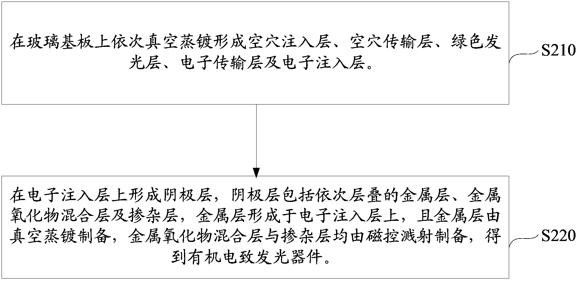
[0044] Such as figure 2 Shown, the preparation method of the organic electroluminescent device of one embodiment, comprises the following steps:
[0045] Step S210: sequentially vacuum-evaporating a hole injection layer, a hole transport layer, a green light emitting layer, an electron transport layer, and an electron injection layer on the glass substrate.
[0046] Preferably, before forming the hole injection layer by vacuum evaporation on the glass substrate, a step of cleaning the glass substrate is also included: cleaning the glass substrate sequentially with detergent, deionized water, acetone and ethanol ultrasonically, and then drying. In a specific embodiment, wash for 5 minutes each time, stop for 5 minutes, repeat 3 times respectively, and then dry in an oven.
[0047] Preferably, the step of activating the surface of the glass substrate is further included after cleaning the glass substrate and before forming the hole injection layer by vacuum evaporation on the ...
Embodiment 1
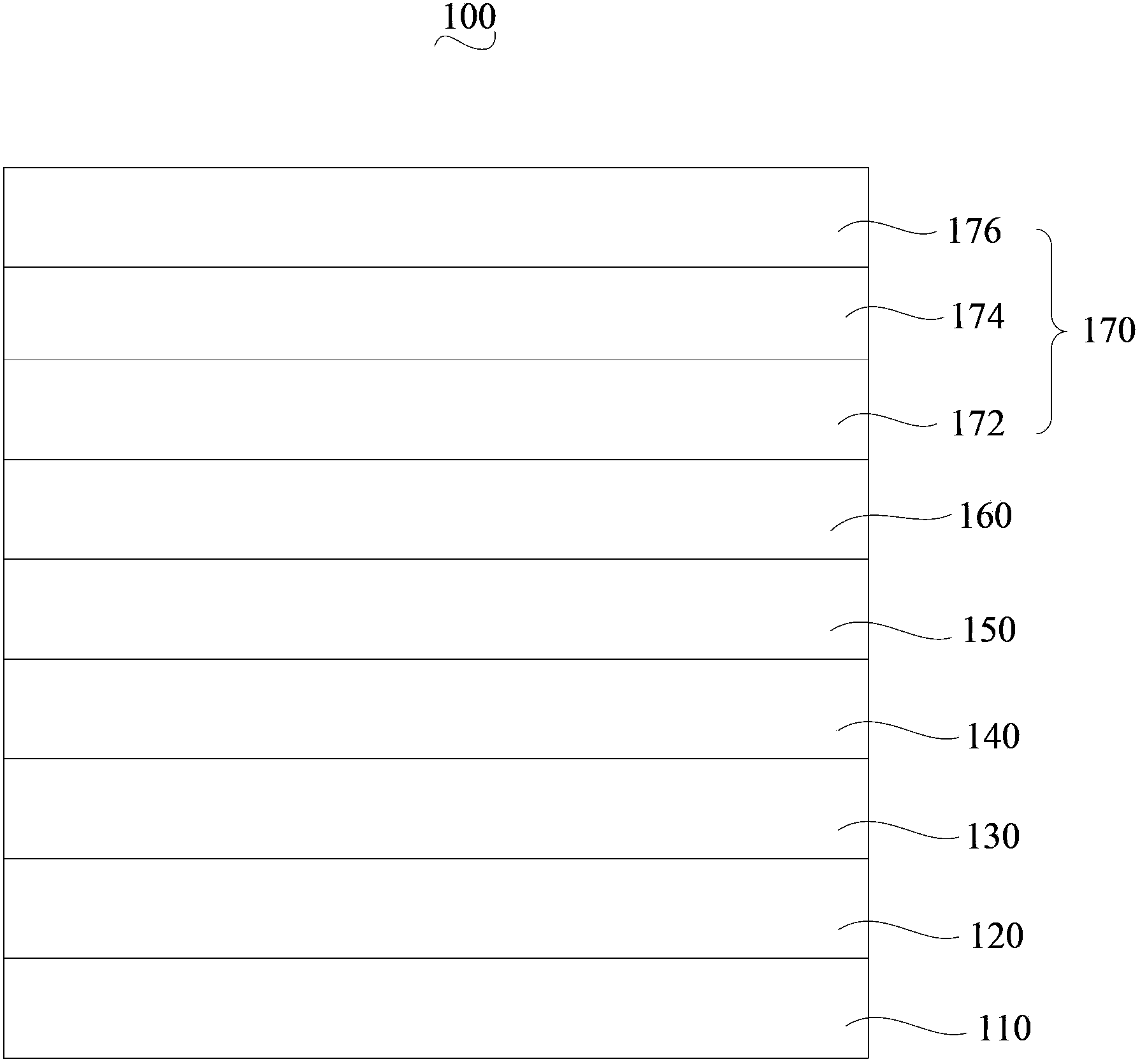
[0060] The structure of the organic electroluminescent device of the present embodiment is: ITO / NPB:MoO 3 / NPB / TCTA:Ir(ppy) 3 / Bphen / Bphen:LiF:Li 2 SO 4 / Al / Nb 2 o 5 :V 2 o 5 / (Mg:Ag):IZO.
[0061] The preparation of the organic electroluminescent device of this embodiment is as follows:
[0062] (1) Clean the ITO glass substrate sequentially with detergent, deionized water, acetone and ethanol ultrasonically, wash for 5 minutes each time, stop for 5 minutes, repeat 3 times respectively, then dry in an oven, and dry the dried glass The substrate is subjected to surface activation treatment; wherein, the thickness of the ITO glass substrate is 100 nanometers.
[0063] (2) Hole injection layer, hole transport layer, green light-emitting layer, electron transport layer and electron injection layer are formed by vacuum evaporation on the glass substrate in sequence: the material of the hole injection layer is molybdenum trioxide (MoO 3 ) doped N,N'-diphenyl-N,N'-di(1-naph...
Embodiment 2
[0067] The structure of the organic electroluminescent device of the present embodiment is: ITO / TCTA:WO 3 / TCTA / mCP:Ir(ppy) 2 (acac) / BCP / BCP:LiN 3 :Na 2 SO 4 / Ni / Ta 2 o 5 :V 2 o 5 / (Al:Li):ITO.
[0068] The preparation of the organic electroluminescent device of this embodiment is as follows:
[0069] (1) Clean the ITO glass substrate sequentially with detergent, deionized water, acetone and ethanol ultrasonically, wash for 5 minutes each time, stop for 5 minutes, repeat 3 times respectively, then dry in an oven, and dry the dried glass The substrate is subjected to surface activation treatment; wherein, the thickness of the ITO glass substrate is 100 nanometers.
[0070] (2) Hole injection layer, hole transport layer, green light-emitting layer, electron transport layer and electron injection layer are formed by vacuum evaporation on the glass substrate in sequence: the material of the hole injection layer is tungsten trioxide (WO 3 ) doped 4,4',4''-tris(carbazol-9-...
PUM
| Property | Measurement | Unit |
|---|---|---|
| Thickness | aaaaa | aaaaa |
| Thickness | aaaaa | aaaaa |
| Thickness | aaaaa | aaaaa |
Abstract
Description
Claims
Application Information