Preparation method of high-accuracy ceramic printed circuit board

A production method and technology of ceramic substrates are applied in the production of conductive lines on the surface of ceramic materials. In the field of producing high-precision conductive lines on the surface of ceramic materials, it can solve problems such as difficult industrial application, and achieve elimination of influence, reduction in width, and good edge quality. Effect

Active Publication Date: 2014-10-15
HUAZHONG UNIV OF SCI & TECH
View PDF8 Cites 16 Cited by
  • Summary
  • Abstract
  • Description
  • Claims
  • Application Information

AI Technical Summary

Problems solved by technology

Therefore, it is difficult to realize the industrial application of highly flexible laser processing technology in the field of ceramic circuit board manufacturing.

Method used


Image

  • Preparation method of high-accuracy ceramic printed circuit board
  • Preparation method of high-accuracy ceramic printed circuit board
  • Preparation method of high-accuracy ceramic printed circuit board

Examples


Embodiment 1

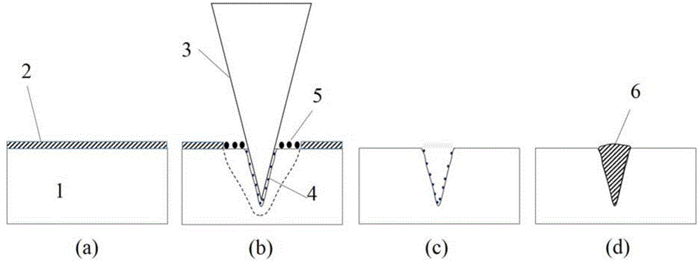
[0039] (1) Soak the 96% alumina ceramic piece as a whole in 1mol / L palladium acetate solution at room temperature for 5 minutes, take it out and dry it.

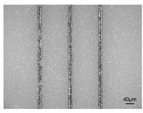
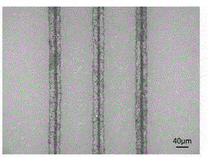
[0040] (2) The alumina ceramic sheet covered with palladium acetate film was modified by ultraviolet nanosecond pulsed laser. The laser source adopts ultraviolet pulse Nd:YVO with a maximum output power of 10W, a pulse width of 20-40ns, a pulse repetition frequency of 25-100kHz, and a wavelength of 355nm. 4 laser. The ceramic sheet is placed on the workbench of a three-axis linkage CNC machine tool and fixed by a negative pressure adsorption device. The laser beam scans the surface of the substrate according to a predetermined line pattern after passing through a beam expander, a scanning galvanometer and an f-theta lens. During laser surface modification, control the laser energy density above the ceramic modification threshold. When the laser output power is 2W (the power density of the laser is 1.13×10 6 W / cm 2), the...

Embodiment 2

[0044] (1) Soak the 99% alumina ceramic piece as a whole in 0.5mol / L palladium chloride solution, the soaking temperature is room temperature, and the soaking time is 5 minutes, take it out and dry it.

[0045] (2) A nanosecond pulsed laser is used to modify the alumina ceramic sheet covered with a palladium chloride thin film. The laser source is a pulsed fiber laser with a maximum output power of 50W, a pulse width of 120ns, a pulse repetition frequency of 50kHz, and a wavelength of 1064nm. The ceramic sheet is placed on the workbench of a three-axis linkage CNC machine tool and fixed by a negative pressure adsorption device. The laser beam scans the surface of the substrate according to a predetermined line pattern after passing through a beam expander, a scanning galvanometer and an f-theta lens. During laser surface modification, control the laser energy density above the ceramic modification threshold. When the laser output power is 10.8W (the power density of the lase...

Embodiment 3

[0049] (1) Coat an aqueous solution containing 0.1 mol / L palladium chloride on the position of the designed circuit pattern on the surface of the aluminum nitride ceramic sheet, and dry it naturally.

[0050] (2) Using ultraviolet nanosecond pulsed laser to modify the aluminum oxide ceramic sheet covered with palladium chloride thin film. The laser source adopts ultraviolet pulse Nd:YVO with a maximum output power of 10W, a pulse width of 20-40ns, a pulse repetition frequency of 25-100kHz, and a wavelength of 355nm. 4 laser. The ceramic sheet is placed on the workbench of a three-axis linkage CNC machine tool and fixed by a negative pressure adsorption device. The laser beam scans the surface of the substrate according to a predetermined line pattern after passing through a beam expander, a scanning galvanometer and an f-theta lens. During laser surface modification, control the laser energy density above the ceramic modification threshold. When the laser output power is 0....


PUM

PropertyMeasurementUnit
wavelengthaaaaaaaaaa
electrical resistivityaaaaaaaaaa

Abstract

The invention discloses a preparation method of a high-accuracy ceramic printed circuit board. The preparation method comprises the steps of radiating laser on the surface of a ceramic substrate covered with a palladium ion solid film, controlling the energy density of the laser to reach above a modified threshold of the substrate, allowing a V-shaped microgroove structure to be formed on the surface of the ceramic substrate, allowing a palladium ion in a microgroove to be reduced to an atom state, bonding the palladium ion with an oxygen atom at a high temperature to form palladium oxide with very high chemical stability, forming firm metallurgical bonding with the substrate, allowing the structure on the surface of the substrate in a heat affected zone of the laser not to be changed, and only allowing the palladium ion to be reduced to metal palladium. Metal palladium in the heat affected zone is selectively removed by the chemical cleaning step; palladium oxide in the microgroove structure is left as an active center of catalytic chemical plating reaction; and then a high-accuracy conducting circuit can be obtained by implementing chemical plating. According to the preparation method, the conducting circuit can be quickly prepared on the surface of the ceramic substrate; the preparation method has no special requirement for a material of the substrate; and the obtained conducting circuit is high in accuracy, good in conductivity and high in binding force.

Description

technical field [0001] The invention belongs to the field of conductive circuit board production and the field of laser surface treatment, and relates to a method for manufacturing high-precision conductive circuits on the surface of ceramic materials. Specifically, laser surface modification technology, chemical cleaning technology and electroless plating technology are used in the production of conductive circuits on the surface of ceramic materials. Background technique [0002] With the rapid popularization of electronic information industries such as computers and the Internet, mobile communications, flat panel displays, solar photovoltaic industry, and energy-saving lighting industry, electronic and electrical products continue to develop in the direction of miniaturization, flexibility, and high integration. Electronic packaging technology has entered a period of ultra-high-speed development. The printed circuit board (PCB) is almost an essential core component of ev...

Claims


Application Information

Patent Timeline
Patent Type & Authority Applications(China)
IPC IPC(8): H05K3/18H05K3/00
Inventor 吕铭曾晓雁刘建国
Owner HUAZHONG UNIV OF SCI & TECH
Why Eureka
Try Eureka