Photoelectrode using metal nitride as conductive substrate and preparation method thereof

A conductive substrate and metallic technology, applied in the field of photoelectrodes, can solve the problems of small photoresponse range, no proposal, high cost of conductive substrate, etc., and achieve the effects of low cost, photoactive layer protection and low resistance

Active Publication Date: 2014-11-05
ZHANGJIAGANG IND TECH RES INST CO LTD DALIAN INST OF CHEM PHYSICS CHINESE ACADEMY OF SCI +1
View PDF13 Cites 24 Cited by
  • Summary
  • Abstract
  • Description
  • Claims
  • Application Information

AI Technical Summary

Problems solved by technology

Wide bandgap oxide semiconductors such as TiO 2 、WO 3 The photoresponse range is small, and sunlight cannot be fully utilized; and narrow-bandgap all-oxide semiconductors often have one or more of the following problems: (1) The position of the conduction band is too low, resulting in insufficient electron reduction, and a large bias is required (such as α -Fe 2 o 3 , BiVO 4 ); (2) The charge separation efficiency of non-full d electrons is not high (such as CaFe 2 o 4 , α-Fe 2 o 3 ); (2) unstable under photoelectrochemical reaction (such as Cu 2 o)
Literature (Adv.Mater.2013, 25, 125) reported that Ta 3 N 5 Photoelectrodes, in NH 3 Ta and Ta 3 N 5 Ta 2 N, but no proposal to adopt such as Ta 2 Nitrides such as N are used as conductive substrates, and semiconductors are not deposited on metallic nitride substrates.
Moreover, the abundance of tantalum in the earth's crust is only 2ppm, and the cost of metal tantalum or tantalum nitride as a conductive substrate is high

Method used


Image

  • Photoelectrode using metal nitride as conductive substrate and preparation method thereof
  • Photoelectrode using metal nitride as conductive substrate and preparation method thereof
  • Photoelectrode using metal nitride as conductive substrate and preparation method thereof

Examples


Embodiment 1

[0018] Preparation of metallic titanium nitride: metal Ti sheet (33mm*20mm2 sheet) is placed in a tube furnace and sealed, evacuated, N 2 Replace 3 times, and then keep the 20sccm N 2 , the temperature of the tube furnace was raised to 600°C at 10°C / min, and then raised to 900°C at 5°C / min, kept for 6 hours and then lowered. Cool to room temperature and take it out to obtain titanium nitride, which is yellow in color, and the measured resistance is 2 ohms at a distance of about 1 cm from the test leads.

Embodiment 2

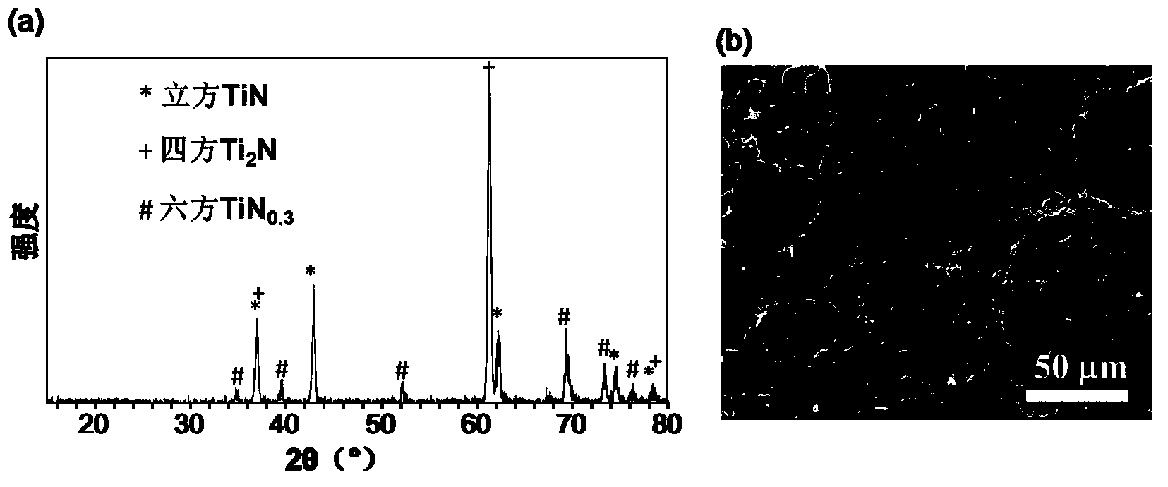
[0020] Preparation of metallic titanium nitride: metal Ti sheet (33mm*20mm2 sheet) is placed in a tube furnace and sealed, evacuated, N 2 Replace 3 times, and then keep the 20sccm N 2 , the temperature of the tube furnace was raised to 600°C at 10°C / min, and then raised to 1000°C at 5°C / min, kept for 6 hours and then cooled down. Cool to room temperature and take it out to obtain titanium nitride, which is yellow in color and darker and brighter than the sample treated at 900°C. figure 1 (a) is the XRD pattern of the prepared sample, showing cubic TiN phase, tetragonal Ti 2 N-phase and hexagonal TiN 0.3 Mutually, figure 1 (b) is the SEM image of the sample surface.

Embodiment 3

[0022] Preparation of metallic titanium nitride: metal Ti sheet (30mm*35mm2 sheet) is placed in a corundum tube furnace and sealed, evacuated, N 2 Replace 3 times, and then keep the 20sccm N 2, the temperature of the tube furnace was raised to 600°C at 20°C / min, then to 900°C at 10°C / min, and then to 1200°C at 5°C / min, kept for 18 hours and then lowered. Cool to room temperature and take out to obtain titanium nitride, which is brown.


PUM

PropertyMeasurementUnit
electrical resistivityaaaaaaaaaa
electrical resistanceaaaaaaaaaa
electrical resistivityaaaaaaaaaa

Abstract

The invention discloses a photoelectrode and a preparation method thereof. A metal nitride substrate serves as a current collection body and is tightly contacted with a photoactive layer which is a non-complete oxide semiconductor with or without the decoration of a promoter, so that the photoelectrochemical photoelectrode is formed. The preparation method comprises the following steps of: firstly, preparing the conductive metal nitride substrate, wherein the lowest sheet resistance of the conductive metal nitride substrate is 1.8 ohm per square, the electrical resistivity is 0.16 mohm per centimeter, the conductive metal nitride substrate is superior to commercial FTO and ITO; and secondarily, depositing or coating the semiconductor or a precursor containing a semiconductor metal constituent, performing high-temperature processing in an inert atmosphere or a hydride atmosphere of the semiconductor nonmetal constituent. The metal nitride substrate can keep conductivity after being subjected to high-temperature processing in the inert or hydride atmosphere (such as to 900 DEG C in ammonia gas), and is applicable for high-temperature preparation process of a non-all oxide semiconductor photoelectrode, and the whole photoelectrode preparation process is easy to industrialize. The photoelectrode can be used for application such as water decomposition, hydrogen preparation and carbon dioxide conversion by means of solar energy in photoelectrochemistry.

Description

technical field [0001] The invention relates to a structure of a photoelectrode for photoelectrochemical process in solar energy utilization and a preparation method thereof. Background technique [0002] With the increasingly prominent energy problems, solar energy, as an abundant clean energy, has been paid more and more attention to the research on its utilization. As an important means of converting and utilizing solar energy, photoelectrochemistry has also made good progress in its research. Fujishima and Honda first reported metal In-connected single crystal TiO 2 The photoelectrode realizes photoelectrochemical water splitting (Nature1972, 238, 37.), which is the first of its kind in the study of photoelectrochemical conversion of light energy. Then many oxide semiconductor materials were developed as photoactive layers, such as WO 3 (Chemical Communications2012, 48, 729-731), ZnO (Adv. Funct. Mater. 2009, 19, 1849-1856), In 2 o 3 (Electrochimica Acta 2000, 45, 1...

Claims


Application Information

Patent Timeline
Patent Type & Authority Applications(China)
IPC IPC(8): H01G9/20H01G9/042
Inventor 李灿熊锋强刘臣王楠
Owner ZHANGJIAGANG IND TECH RES INST CO LTD DALIAN INST OF CHEM PHYSICS CHINESE ACADEMY OF SCI
Why Eureka
Try Eureka