
Electrically erasable programmable read-only memory (EEPROM)

A storage unit and capacitor technology, applied in electrical components, electric solid devices, circuits, etc., can solve problems such as unfavorable chip working field strength, information loss, wrong writing, etc., to improve data storage capabilities, improve data storage capabilities, The effect of operating voltage reduction

Active Publication Date: 2014-11-19
合肥矽景电子有限责任公司
View PDF3 Cites 0 Cited by
  • Summary
  • Abstract
  • Description
  • Claims
  • Application Information

AI Technical Summary

Problems solved by technology

Existing EEPROM consumes a lot of power because its gate structure is a vertical stack structure composed of polysilicon control gate, coupling oxide layer, polysilicon floating gate and tunnel oxide layer. The problems brought by this structure are: 1. Make the EEPROM The working voltage of the chip is high, which is not conducive to reducing the working field strength of the chip and increasing the reading and writing distance; 2. EEPROM is used as the information carrier of the RFID tag chip, because the capacitance value of the existing stack structure is small, sometimes in the work, with When the working distance and angle change, there is a possibility of power failure in the middle, which will cause information loss or wrong writing

Method used


Image

  • Electrically erasable programmable read-only memory (EEPROM)
  • Electrically erasable programmable read-only memory (EEPROM)
  • Electrically erasable programmable read-only memory (EEPROM)

Examples


Embodiment 1

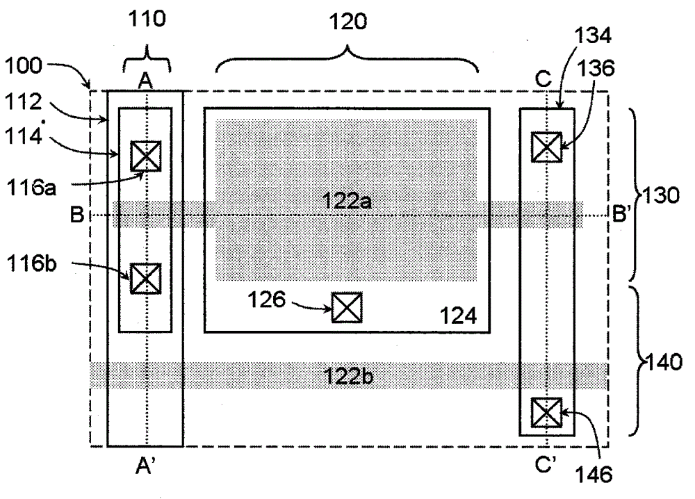
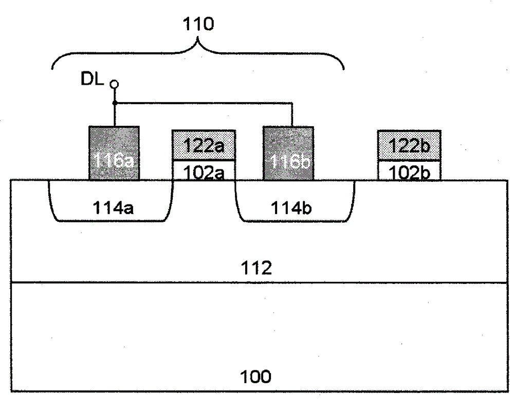
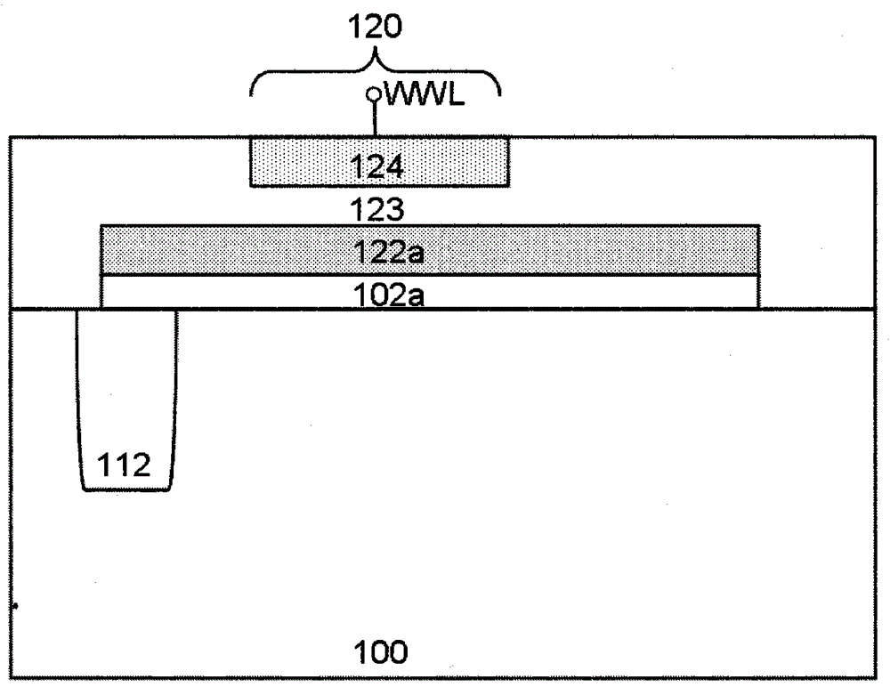
[0020] Such as figure 1 A kind of EEPROM storage unit shown, described semiconductor substrate is the epitaxial silicon slice 100 of P-type doping, the PMOS electric capacity 110, polysilicon electric capacity 120, NMOS selector tube 130, NMOS reading tube 140 formed on the semiconductor substrate; The PMOS capacitor 110 includes: an n-well 112 formed by ion implantation on a p-type doped epitaxial silicon wafer 100, a first gate oxide layer 102a, a second gate oxide layer 102b, a floating gate 122a placed on the first gate oxide layer 102a, a source drain Region one 114a, source drain region two 114b, MOS capacitor contact hole one 116a placed on source drain region one 114a and MOS capacitor contact hole two 116b placed on source drain region two 114b, the floating gate 122a is used as a PMOS capacitor The first MOS capacitor contact hole 116a and the second MOS capacitor contact hole 116b are short-circuited for connecting DL, and the first source-drain region 114a and the ...


PUM


Abstract

The present invention discloses an EEPROM structure. The EEPROM structure belongs to the semiconductor manufacture technology field, and comprises a semiconductor substrate, and a metal oxide semiconductor (MOS) capacitor, a polysilicon capacitor, an MOS selectron and an MOS reading tube which are formed on the semiconductor substrate. The capacitance value of the polysilicon capacitor is greater than the capacitance value of the MOS capacitor. The EEPROM structure is low in working voltage, thereby being able to improve the data storage capability, and possessing the high reliability, durability and data security.

Description

technical field [0001] The invention relates to a semiconductor storage device, in particular to an EEPROM storage device. Background technique [0002] RFID tags have been widely used in goods supply management, package tracking and identification, logistics warehousing, mobile commerce, aviation and medical services. The passive RFID tag chip includes radio frequency, logic and memory modules, where the memory module provides information storage space for product identification, transmission, catalog list and user information. In the prior art, EEPROM has a competitive advantage over Ferroelectric Random Access Memory (FeRAM) in terms of read operation, because its read operation does not destroy information and does not need to be rewritten after reading. In addition, its compatibility with the CMOS process is also better than the latter, which is convenient for large-scale industrial production and helps reduce costs. [0003] The passive RFID tag chip has no power sup...

Claims


Application Information

Patent Timeline
IPC IPC(8): H01L27/115
Inventor 陈龙
Owner 合肥矽景电子有限责任公司
Features
  • Generate Ideas
  • Intellectual Property
  • Life Sciences
  • Materials
  • Tech Scout
  • Unparalleled Data Quality
  • Higher Quality Content
  • 60% Fewer Hallucinations
Learn More