Preparation method of large-area transparent conducting film glass
A transparent conductive film and transparent conductive technology, applied in the direction of coating, etc., can solve the problems of difficult control and complicated process, and achieve the effects of easy operation, simple process, and low cost of equipment and raw materials
- Summary
- Abstract
- Description
- Claims
- Application Information
AI Technical Summary
Problems solved by technology
Method used
Image
Examples
Embodiment 1
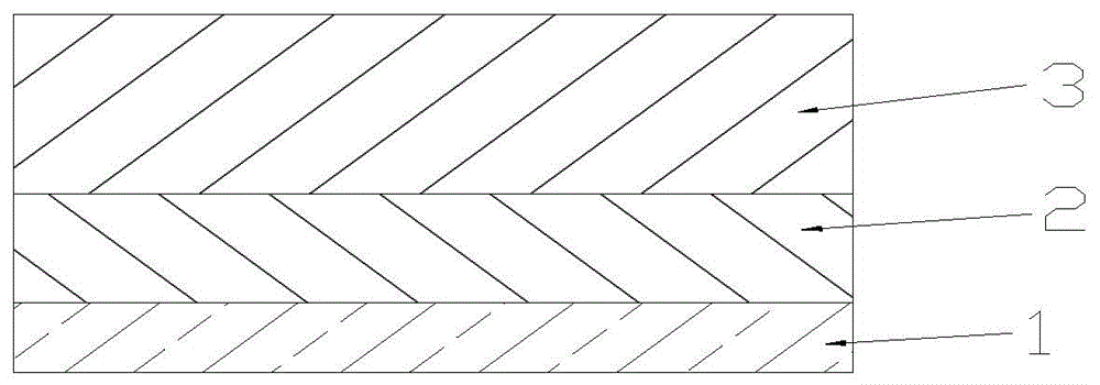
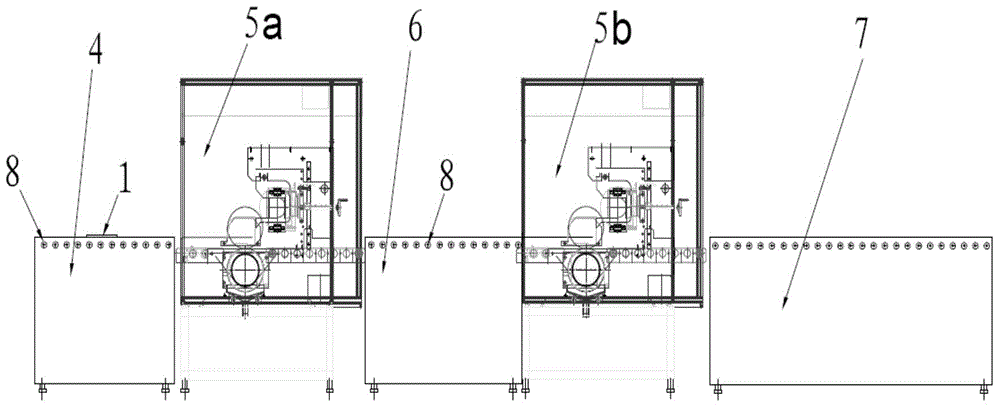
[0035] In this embodiment, the glass substrate is 3.2mm ultra-clear glass; using the first liquid phase roll coater, a silicon dioxide interlayer film is plated on the glass surface with tetraethyl orthosilicate hydrolysis precursor; Then, the mixed solution of tin tetrachloride and ammonium fluoride (ethanol as a solvent) is coated on the glass surface by using the second liquid-phase roller coater reactor to form a tin oxide-doped fluorine (FTO) transparent conductive film. The post-treatment temperature of the glass substrate is 560°C, and the post-treatment time is 10 minutes;
[0036]After measurement, the thickness of the middle layer is 85nm, the thickness of the FTO transparent conductive layer is 670nm, the sheet resistance of the film layer is 7.6Ω / □, and the carrier concentration of the film layer is n is 7.8×10 20 / cm 3 , The visible light transmittance of FTO transparent conductive film glass is 82%. Therefore, it can be seen that the FTO transparent conductive ...
Embodiment 2
[0038] In the present embodiment, the glass substrate is 4mm ultra-clear glass; utilize the first liquid-phase roller coater to coat a layer of silicon dioxide interlayer film on the glass surface with the hydrolysis precursor solution of methyl orthosilicate; then The mixed solution of monobutyltin trichloride and antimony trichloride (the mixture of propanol and water is the solvent) is coated on the glass surface by using the second liquid phase roller coater reactor to form tin oxide doped with antimony (ATO) transparent conductive film. The post-treatment temperature of the glass substrate is 580°C, and the post-treatment time is 12 minutes;
[0039] After measurement, the thickness of the middle layer is 106nm, the thickness of the ATO transparent conductive layer is 710nm, the square resistance of the film layer is 7.0Ω / □, the carrier concentration of the film layer is 8.1×10²⁰ / cm3, the ATO transparent conductive film glass Visible light transmittance is 79%. Therefor...
PUM
| Property | Measurement | Unit |
|---|---|---|
| thickness | aaaaa | aaaaa |
| thickness | aaaaa | aaaaa |
| electrical resistivity | aaaaa | aaaaa |
Abstract
Description
Claims
Application Information

