A kind of preparation method of semiconductor laser cavity mirror

A laser and semiconductor technology, which is applied in the direction of semiconductor lasers, lasers, laser components, etc., can solve the problems of high binding energy of the surface layer, excessive ion beam energy, surface damage, etc., and achieve high production efficiency, reduce contamination, and effectively The effect of surface states

Active Publication Date: 2017-09-26
XIAN LIXIN PHOTOELECTRIC SCI & TECH
View PDF6 Cites 0 Cited by
  • Summary
  • Abstract
  • Description
  • Claims
  • Application Information

AI Technical Summary

Problems solved by technology

This technology is not good in actual effect. The main reason is that the surface layer has a high binding energy, and it is difficult to remove it by physical bombardment. In addition, the excessive energy of the ion beam will cause damage to the surface, which is not conducive to improving COMD.

Method used


Image

  • A kind of preparation method of semiconductor laser cavity mirror
  • A kind of preparation method of semiconductor laser cavity mirror

Examples


preparation example Construction

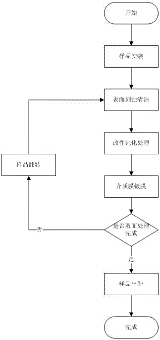
[0045] A method for preparing a semiconductor laser cavity mirror, comprising the following steps:

[0046] Step 1, surface cleaning;

[0047] Step 2, surface modification and passivation;

[0048] Step 3, dielectric coating;

[0049] Step 4, turn over, repeat steps 1 to 3, remove.

Embodiment 1

[0051] Such as figure 1 The specific steps of surface cleaning in the described step one are as follows:

[0052] Surface cleaning:

[0053] (2.1) Put the sample of semiconductor laser cavity mirror into the vacuum cavity and fix it on the sample holder;

[0054] (2.2) Adjust the direction of one of the two end faces of the sample to the same direction as that of the plasma cleaning treatment;

[0055] (2.3) Vacuumize the cavity, and the air pressure in the cavity reaches 10 -5 Pa or 10 -6 Pa;

[0056] (2.4) Adjust the temperature of the sample to 350°C or 400°C or 450°C, and feed inert gas into the vacuum chamber, adjust the air pressure in the vacuum chamber to keep the air pressure within the range of 1-10torr, and activate the vacuum chamber Plasma, to stabilize the plasma state, clean the adsorbate on the surface of the sample by fluoride or argon plasma;

[0057] (2.5) Use electric heating or infrared lamps and thermocouple feedback to control the sample temperatur...

Embodiment 2

[0075] Surface cleaning:

[0076] (2.1) Put the sample of semiconductor laser cavity mirror into the vacuum cavity and fix it on the sample holder;

[0077] (2.2) Adjust the direction of one of the two end faces of the sample to the same direction as that of the plasma cleaning treatment;

[0078] (2.3) Vacuumize the cavity, and the air pressure in the cavity reaches 10 -6 Pa; the air pressure after vacuuming is more suitable for cleaning the surface of the sample;

[0079] (2.4) Adjust the temperature of the sample to 400°C, and feed inert gas into the vacuum chamber, adjust the air pressure in the vacuum chamber to keep the air pressure at 10torr, activate the plasma in the vacuum chamber, wait for the plasma state to stabilize, and Clean up the adsorbate on the surface of the sample; if the temperature is too high or the pressure is too high, the inert gas will lose its function; if the temperature or pressure is too low, the plasma will not be activated;

[0080] (2.5) ...


PUM


Abstract

The invention belongs to the technical field of semiconductor surface modification, and specifically relates to a method for preparing a semiconductor laser cavity mirror, comprising the following steps: Step 1, cleaning; Step 2, passivation modification; Step 3, dielectric film coating; Step 4, flipping, Repeat step 1 to step 3, step 5, remove; the semiconductor laser cavity mirror modification method can be compatible with chemical and physical surface modification technology, which improves the selectivity and integrity of surface treatment; makes the surface clean and passivation modified The dielectric film coating of the double-sided cavity mirror is completed in the same vacuum chamber at one time, which reduces the number of sample entry and exit operations and possible pollution and damage, improves the cost rate, and greatly improves production efficiency; this method is based on the same equipment. Surface cleaning, modified passivation and dielectric film technology are integrated on the surface, so that the various steps of surface treatment are seamlessly connected, and the performance and yield of the finished product are improved; further, the treatment of the double-sided dielectric film cavity mirror is also completed in one step. The production efficiency and quality stability are further enhanced; the method is suitable for batch processing, has high production efficiency and low comprehensive cost.

Description

technical field [0001] The invention belongs to the technical field of material surface modification and coating, and in particular relates to a method for preparing a semiconductor laser cavity mirror. Background technique [0002] The structure of the semiconductor laser chip has three main components: the semiconductor gain medium, the laser resonant cavity, and the driving electrode. Judging from the current technology of laser chips, these three parts have certain mature design and manufacturing technologies. Such as semiconductor energy band design and epitaxial growth technology, end face treatment technology of resonant cavity, and ohmic electrode contact growth technology. These technologies push the performance of semiconductor laser chips toward wider wavelength bands, higher brightness and power, higher efficiency, higher reliability and longer life. [0003] At present, the energy density of high-power lasers has reached the order of 100 megawatts per square c...

Claims


Application Information

Patent Timeline
Patent Type & Authority Patents(China)
IPC IPC(8): H01S5/028C23C14/22
Inventor 吴建耀宋克昌杨国文
Owner XIAN LIXIN PHOTOELECTRIC SCI & TECH
Why Eureka
Try Eureka