High-detectivity gallium-nitride-based Schottky ultraviolet detector using graphene

An ultraviolet detector, GaN-based technology, applied in the direction of semiconductor devices, electrical components, circuits, etc., can solve the problems of unsatisfactory metal materials, fixed work function, and decreased light transmittance, so as to enhance the built-in electric potential field, Effect of increasing responsivity and increasing quantum efficiency

Active Publication Date: 2015-03-04
BEIJING UNIV OF TECH
View PDF11 Cites 16 Cited by
  • Summary
  • Abstract
  • Description
  • Claims
  • Application Information

AI Technical Summary

Problems solved by technology

[0004] Traditional Schottky-type devices mainly use translucent metals, but the translucent metal Ni/Au (2nm/2nm) usually used as a Schottky contact has a light transmittance of only about 60% at 300nm, which affects the detection rate. very serious
Studies have shown that f

Method used


Image

  • High-detectivity gallium-nitride-based Schottky ultraviolet detector using graphene
  • High-detectivity gallium-nitride-based Schottky ultraviolet detector using graphene
  • High-detectivity gallium-nitride-based Schottky ultraviolet detector using graphene

Examples


Example Embodiment

[0028] Example 1

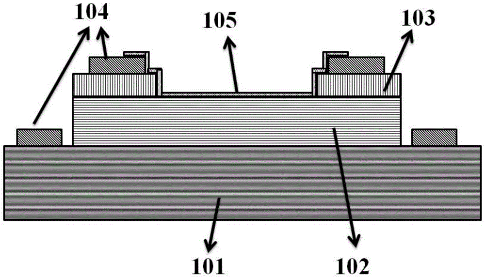
[0029] Step 1. Use metal-organic chemical vapor deposition (or molecular beam epitaxy system, liquid phase epitaxy technology, etc.) to sequentially fabricate heavily doped n-type gallium nitride 101, lightly doped hetero n-type gallium nitride 102 .

[0030] Step 2, cleaning the epitaxial wafer, photolithography, and etching to form a mesa structure, such as heavily doped n-type GaN 101 and lightly doped n-type GaN 102 .

[0031] Step 3, growing a layer of silicon dioxide, and performing photolithography and etching to form a silicon dioxide insulating layer 103 .

[0032] Step 4, photoetching the electrode pattern, sputtering or evaporating to make the metal electrode 104 .

[0033] Step 5, transfer the graphene to the surface of the device, photolithographically etch the graphene pattern, and plasma etch the graphene to form a graphene film 105 . The plasma etching gas is oxygen, the flow rate is 10-70L / min, the power is 50-100W, and the etching time i...

Example Embodiment

[0037] Example 2

[0038] Step 1. Use metal-organic chemical vapor deposition (or molecular beam epitaxy system, liquid phase epitaxy technology, etc.) to sequentially fabricate heavily doped n-type GaN 101 on sapphire (or silicon wafer, silicon carbide, etc. substrates), lightly doped hetero n-type gallium nitride 102 .

[0039] Step 2, using inductively coupled plasma etching to etch the surface of the epitaxial wafer, the etching depth is 10-50 nm, and increasing the defect density on the surface of the epitaxial wafer.

[0040] Step 3: Clean the epitaxial wafer, perform photolithography, and etch to form a mesa structure, such as heavily doped n-type GaN 101 and lightly doped n-type GaN 102 .

[0041] Step 4, growing a layer of silicon dioxide, and performing photolithography and etching to form a silicon dioxide insulating layer 103 .

[0042] Step 5, photoetching the electrode pattern, sputtering or evaporating to make the metal electrode 104 .

[0043]Step 6, transfe...


PUM

PropertyMeasurementUnit
Thicknessaaaaaaaaaa
Thicknessaaaaaaaaaa

Abstract

The invention provides a high-detectivity gallium-nitride-based Schottky ultraviolet detector using graphene. According to the basic structure, the high-detectivity gallium-nitride-based Schottky ultraviolet detector sequentially comprises heavily-doped n type gallium nitride, slightly-doped n type gallium nitride, a silicon dioxide insulating layer, metal electrodes and a graphene thin film from bottom to top. The metal electrodes have the transparent and electric conduction properties and have the half-metallic property. Under the condition that the metal electrodes make direct contact with the slightly-doped n type GaN, the potential barriers of about 0.5 ev can be formed. The formed potential barriers show that the portions, close to the metal electrodes, in the GaN can be bent, so that a spatial charge area is formed, the electron holes are separated, and the photoproduction electrodynamic potential and the photoproduction current are generated. The responsibility of the detector can be greatly improved by introducing the surface defect method. The high-detectivity gallium-nitride-based Schottky ultraviolet detector is simple in structure and process and high in efficiency; thus, the electron hole pair separation capacity is increased, the internal quantum efficiency of the detector is increased, and the detectivity and responsibility are increased.

Description

technical field [0001] The invention relates to a novel GaN-based Schottky type ultraviolet detector structure and preparation method, belonging to the technical field of semiconductor optoelectronic devices. Background technique [0002] There are many applications of ultraviolet detection technology, which can be used for resin curing of polymeric materials, water purification treatment, flame detection, biological effects, and environmental pollution monitoring and ultraviolet light storage. In terms of ultraviolet photodetection devices, GaN materials have excellent performance: (1) GaN does not absorb visible light, and the ultraviolet detectors made can be blinded to visible light and do not require a filter system. (2) No need to make shallow junctions, This can greatly improve the quantum efficiency. (3) GaN has strong anti-radiation ability and can play a role in exploring the mysteries of the universe. GaN ultraviolet detectors are currently mainly divided into th...

Claims


Application Information

Patent Timeline
IPC IPC(8): H01L31/108
CPCH01L31/108H01L31/18
Inventor 徐晨许坤孙捷邓军朱彦旭解意洋荀孟
Owner BEIJING UNIV OF TECH
Why Eureka
Try Eureka