
High detection rate GaN-based Schottky ultraviolet detector using graphene
An ultraviolet detector, gallium nitride-based technology, applied in the direction of semiconductor devices, electrical components, circuits, etc., can solve the problems of unsatisfactory metal materials, detection rate impact, light transmittance drop, etc., to enhance the built-in electric potential field, The effect of increasing the detection rate and responsivity and increasing the quantum efficiency
Patent Information
- Authority / Receiving Office
- CN · China
- Patent Type
- Patents(China)
- Current Assignee / Owner
- Publication Date
- 2017-02-01
Smart Images
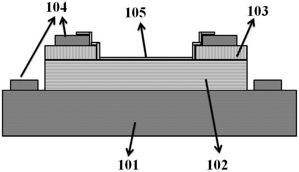
Figure 1 
Figure 2 
Figure 3
Abstract
Description
Technical field
[0001] The invention relates to a novel gallium nitride-based Schottky-type ultraviolet detector structure and preparation method, and belongs to the technical field of semiconductor optoelectronic devices. Background technique
[0002] Ultraviolet detection technology has many applications, which can be used for polymer resin curing, water purification treatment, flame detection, biological effects, environmental pollution monitoring, and ultraviolet light storage. In terms of ultraviolet photodetectors, GaN materials have excellent properties: (1) GaN does not absorb visible light, and the made ultraviolet detectors can achieve visible light blindness without a filter system. (2) There is no need to make a shallow junction, This can greatly improve the quantum efficiency. (3) GaN has strong radiation resistance and can play a role in exploring the mysteries of the universe. GaN ultraviolet detectors are currently divided into the following types: photoconductiv...
Examples
Embodiment 1
[0029] Step 1. Use metal organic chemical vapor deposition (or molecular beam epitaxy system, liquid phase epitaxy technology, etc.) to sequentially produce heavily doped n-type gallium nitride 101 and lightly doped sapphire (or silicon wafer, silicon carbide, etc.) Hetero n-type gallium nitride 102.
[0030] Step 2. Cleaning, photolithography, and etching of the epitaxial wafer to form a mesa structure, such as heavily doped n-type gallium nitride 101 and lightly doped n-type gallium nitride 102.
[0031] Step 3: Growing a layer of silicon dioxide, and performing photolithography and etching to form a silicon dioxide insulating layer 103.
[0032] Step 4. Photoetch the electrode pattern, sputter or evaporate to produce the metal electrode 104.
[0033] Step 5: Transfer graphene to the surface of the device, photoetch the graphene pattern, and plasma etch the graphene to form a graphene film 105. The plasma etching gas is oxygen, the flow rate is 10-70L / min, the power is 50-100W, and...
Embodiment 2
[0038] Step 1. Use metal organic chemical vapor deposition (or molecular beam epitaxy system, liquid phase epitaxy technology, etc.) to sequentially fabricate heavily doped n-type gallium nitride 101 on sapphire (or silicon wafer, silicon carbide, etc.), lightly doped Hetero n-type gallium nitride 102.
[0039] Step 2. Use inductively coupled plasma to etch the surface of the epitaxial wafer to an etching depth of 10-50 nm to increase the surface defect density of the epitaxial wafer.
[0040] Step 3. Cleaning, photolithography, and etching of the epitaxial wafer to form a mesa structure, such as heavily doped n-type gallium nitride 101 and lightly doped n-type gallium nitride 102.
[0041] Step 4. Grow a layer of silicon dioxide, and perform photolithography and etching to form a silicon dioxide insulating layer 103.
[0042] Step 5. Photoetch the electrode pattern, sputter or evaporate to produce the metal electrode 104.
[0043] Step 6, transferring graphene to the surface of the de...