Plastic fiber surface plasma sensor based on bimetallic grating and application thereof
A surface plasmon and plastic optical fiber technology, applied in the field of sensors, can solve the problems of low contrast, poor stability, and low excitation efficiency, and achieve high productivity, low cost, and simple production
- Summary
- Abstract
- Description
- Claims
- Application Information
AI Technical Summary
Problems solved by technology
Method used
Image
Examples
Embodiment 1
[0033] A plastic optical fiber surface plasmon sensor based on a double metal grating, comprising a plastic optical fiber as a substrate and a double-layer metal grating arranged on the upper surface and the lower surface of the optical fiber;
[0034] The plastic optical fiber is a plastic optical fiber with cladding removed and a core diameter of 1 mm;
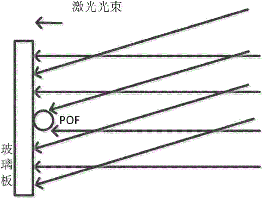
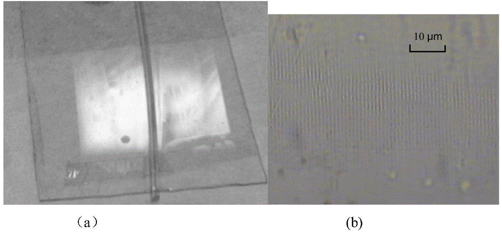
[0035] The double-layer metal grating includes a medium layer with a concave-convex periodic structure on one side, and a metal thin film layer is arranged on the upper surface of the concave-convex periodic structure to form a grating; wherein the duty ratio of the formed grating is 1; The space ratio is a commonly used term in the field, that is, for each grating period, the ratio of the width of the convex part to the concave part is the same; wherein, the double-layer metal grating uses laser double-beam interference light according to the prior art The vertical distance difference between layers in the structure of the ...
Embodiment 2
[0039] A plastic optical fiber surface plasmon sensor based on a double metal grating as described in Example 1, the difference is that the plastic optical fiber is an EL2100 plastic optical fiber produced by Mitsubishi Corporation.
[0040] The parameters of the plastic optical fiber: the geometric size is 980 / 1000 μm; the core refractive index is 1.49, the core numerical aperture (NA) is 0.5, the cladding refractive index is 1.4, and the light transmittance / %*m -1 ≥95(570nm), loss / dB*km -1 ≤200(570nm).
Embodiment 3
[0042] A plastic optical fiber surface plasmon sensor based on a double metal grating as described in Embodiment 1 and 2, the difference is that the metal thin film layer is an aluminum thin film with a thickness of 100 nm. The aluminum thin film is formed by depositing aluminum on the surface of the concave-convex structure of the dielectric layer by using an electron beam depositor, and then cloning the required double-layer metal grating.
PUM
| Property | Measurement | Unit |
|---|---|---|
| diameter | aaaaa | aaaaa |
| size | aaaaa | aaaaa |
| thickness | aaaaa | aaaaa |
Abstract
Description
Claims
Application Information


