Terminal passivation structure for SiC power device and preparation method thereof
A technology of power devices and terminals, which is applied in semiconductor/solid-state device manufacturing, electric solid-state devices, semiconductor devices, etc., can solve the problems of difficult preparation of passivation structures, high temperature resistance, and complicated terminal passivation structures, etc. Good breakdown electricity, high temperature stability, and flexible formation methods
- Summary
- Abstract
- Description
- Claims
- Application Information
AI Technical Summary
Problems solved by technology
Method used
Image
Examples
Embodiment 1
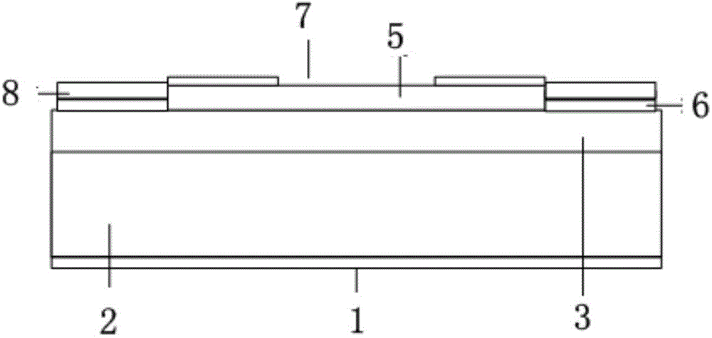
[0040] Such as figure 1 As shown, a terminal passivation structure for SiC power devices includes a SiC substrate layer 2, an ohmic contact layer 1 disposed on one side of the SiC substrate layer 2, and a SiC epitaxial layer 3 disposed on the other side of the SiC substrate layer 2 , the Schottky contact layer 5 located in the middle above the SiC epitaxial layer 3, the silicon oxide layer 6 located on the SiC epitaxial layer 3 and at the periphery of the Schottky contact layer 5; on the silicon oxide layer 6 and the The DLC film layer 8 is provided on the Schottky contact layer 5 , and the DLC film layer 8 on the Schottky contact layer 5 is provided with an opening 7 for exposing the Schottky contact layer 5 . The thickness of the DLC film layer 8 is 150nm-200nm.
Embodiment 2
[0041] Embodiment 2 preparation method
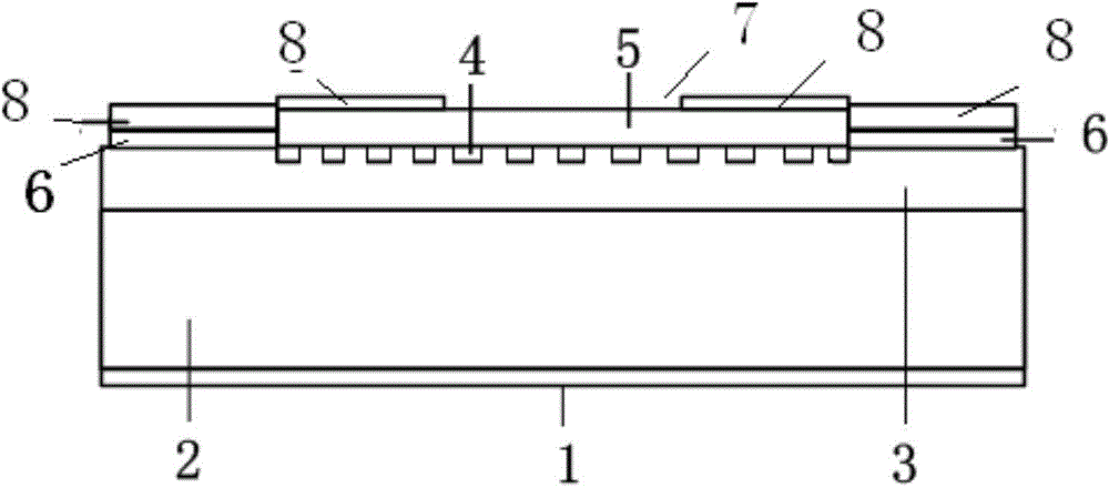
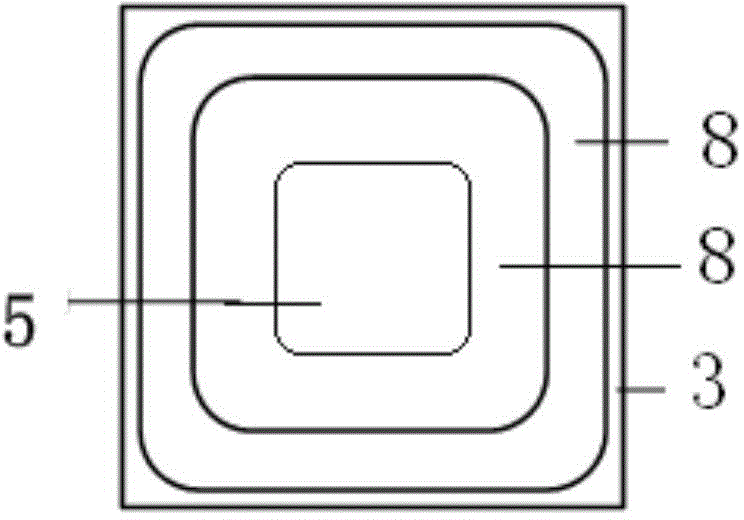
[0042] A cross-sectional schematic diagram of a SiC device using this scheme is shown in figure 2 with 3 Shown (taking the diode device as an example). Form an epitaxial layer on the SiC substrate by epitaxial growth; then form a P-type region by ion implantation; form a silicon oxide layer by in-situ sacrificial oxidation and deposition, and then remove it by photolithography and etching Partial oxidation layer; form ohmic contact on the substrate side; form Schottky contact on the epitaxial layer side; form large-area DLC film on the outside of the Schottky contact; expose the anode metal electrode by etching.
[0043] Taking SiC Schottky diode as an example to illustrate the process of realizing the present invention, such as Figure 4 Shown:
[0044] ① Complete the Schottky contact of the device. The Schottky contact can use multiple metals (such as metal Ti) and a combination of multiple metals, with a thickness of It can b...
PUM
| Property | Measurement | Unit |
|---|---|---|
| Thickness | aaaaa | aaaaa |
| Thickness | aaaaa | aaaaa |
| Thickness | aaaaa | aaaaa |
Abstract
Description
Claims
Application Information


