Method for controllably removing residual optical photoresist in graphene-metal contact region

A technology of metal contact and photoresist, which is applied in the manufacture of electrical components, circuits, semiconductors/solid-state devices, etc., can solve the problems of discounting graphene's electrical properties, restricting application development, hindering the contact between metal and graphene, and reducing doping Effects of complexity, high carrier mobility, and device performance

Inactive Publication Date: 2015-03-25
INST OF MICROELECTRONICS CHINESE ACAD OF SCI
View PDF3 Cites 4 Cited by
  • Summary
  • Abstract
  • Description
  • Claims
  • Application Information

AI Technical Summary

Problems solved by technology

In the preparation process of graphene field effect transistors, in order to define graphics, it is inevitable to use photoresist on the surface of graphene. After exposure and development, a large amount of photoresist remains on the surface of graphene, which hinders the contact between metal and graphene. The introduction of additional potential barriers at the contact interface leads to a great reduction in the electrical properties of graphene, which is one of the bottlenecks that limit its further application development.

Method used


Image

  • Method for controllably removing residual optical photoresist in graphene-metal contact region
  • Method for controllably removing residual optical photoresist in graphene-metal contact region
  • Method for controllably removing residual optical photoresist in graphene-metal contact region

Examples


Embodiment 1

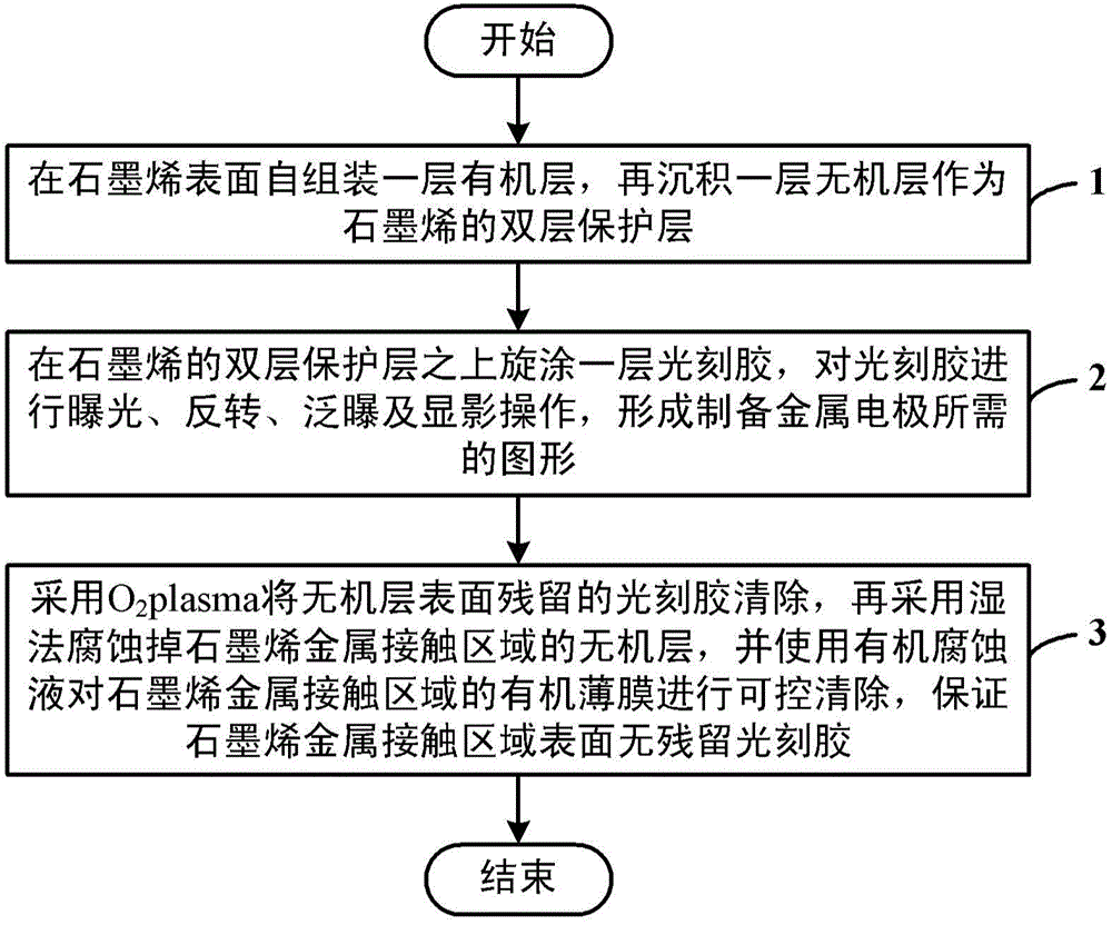
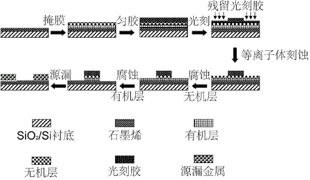
[0042] Embodiment 1. Using polystyrene as the organic layer and metallic nickel as the inorganic layer as the double-shielding layer, the controllable removal of the residual optical photoresist in the double-layer graphene-metal contact area.

[0043] Specific steps are as follows:

[0044] Step 1: Grow a single layer of uniform graphene on the surface of copper foil by CVD method, spin-coat PMMA photoresist on the surface of graphene and heat and bake to cure the photoresist, and then place the copper sheet with graphene and PMMA into a copper etching solution, etch away the copper and transfer it to a silicon dioxide semiconductor substrate with a 300 nm insulating layer.

[0045] Step 2: On 300nm SiO spread with graphene (transferred twice) 2 Spin-coat a layer of 9912 photoresist with a thickness of 1.4 μm on the surface of / Si substrate, after exposure (light intensity 5, time 15s), development (40s), primer, acetone to remove the glue, and graphene into the active area ...

Embodiment 2

[0053] Embodiment 2, using polystyrene as the organic layer, metal nickel as the inorganic layer as the double shielding layer, controllably removes the residual optical photoresist in the graphene-metal contact area.

[0054] The specific steps are similar to those in Example 1, but in step 3, the thickness of polystyrene is 20nm, and the corrosion rate is 1nm / min; in step 4, the thickness of metal nickel is 20nm, and the corrosion rate is 1nm / min.

[0055] Image 6 Be the optical picture in the removal process in embodiment 2, Image 6 The optical photos show that the corrosion rate of the protective layer plays a decisive role in maintaining the integrity of the photolithographic pattern. If the corrosion rate is too fast, the capillary phenomenon is relatively obvious, resulting in the loss of the photolithographic pattern.

Embodiment 3

[0056] Embodiment 3, using polyethylene as the organic layer and metal nickel as the inorganic layer as the double shielding layer, controllably removes the residual optical photoresist in the graphene-metal contact area.

[0057] The specific steps are similar to Example 1, but step 3 uses polyethylene as an organic mask layer with a thickness of 20nm and an etching rate of 1nm / min. In step 4, the thickness of metal nickel is 20nm and the etching rate is 1nm / min.

[0058] Figure 7 For the electrical characteristics of graphene field effect transistor in embodiment 3, Figure 7 The transfer curve shows that the corrosion rate is too fast and the device performance is not good.


PUM

PropertyMeasurementUnit
thicknessaaaaaaaaaa
thicknessaaaaaaaaaa
thicknessaaaaaaaaaa

Abstract

The invention discloses a method for controllably removing residual optical photoresist in a graphene-metal contact region. The method includes the steps that an organic layer is self-assembled on the surface of graphene, an inorganic layer is deposited, and the organic layer and the inorganic layer serve as double protective layers of graphene; the double protective layers of graphene are spin-coated with a layer of photoresist, the photoresist is exposed, reversely rotated, flooded and developed, and patterns needed for manufacturing a metal electrode are formed; residual photoresist on the surface of the inorganic layer is removed through O2 plasma, the portion, in the graphene-metal contact region, of the inorganic layer is etched away through a wet method, the portion, in the graphene-metal contact region, of an organic thin film is controllably removed through organic corrosive liquid, and it is guaranteed that no residual photoresist exists on the surface of the graphene-metal contact region. The problem that the photoresist is prone to be left on the surface of graphene is solved, graphene is not damaged, the doping degree of graphene is reduced, and an established graphene field effect transistor can keep the high carrier mobility of graphene materials and the performance of a device.

Description

technical field [0001] The invention belongs to the technical field of graphene field-effect transistor manufacture, and in particular relates to a method for controllably removing residual optical photoresist in a graphene-metal contact region. Background technique [0002] As integrated circuit technology enters the nanometer scale, key technologies are approaching the physical limit dominated by quantum effects, and the difficulty and cost of the process are increasing sharply. The sustainable development of integrated circuits is facing unprecedented challenges. High speed and low power consumption are key technical bottlenecks in the development of integrated circuits, and both are related to carrier mobility. Finding materials with higher mobility to replace the existing silicon channel has become a very urgent task to further extend Moore's Law. High-mobility carbon materials represented by graphene have attracted widespread attention and have broad application prosp...

Claims


Application Information

Patent Timeline
Patent Type & Authority Applications(China)
IPC IPC(8): H01L21/02H01L21/04
CPCH01L21/0337H01L21/04
Inventor 金智彭松昂史敬元王少青王选芸张大勇
Owner INST OF MICROELECTRONICS CHINESE ACAD OF SCI
Why Eureka
Try Eureka