Manufacturing method and in-situ characterizing method for graphene field effect transistor free of residual optical photoresist

A graphene surface and graphene technology, applied in the field of in-situ characterization of graphene FET, can solve problems such as difficult to meet actual needs, achieve high carrier mobility and device performance, reduce doping degree, and reduce device performance Effect

Active Publication Date: 2015-03-25
INST OF MICROELECTRONICS CHINESE ACAD OF SCI
View PDF5 Cites 9 Cited by
  • Summary
  • Abstract
  • Description
  • Claims
  • Application Information

AI Technical Summary

Problems solved by technology

However, there are few research reports on the surface photoresist removal technology in the process of graphene field effect transistor. needs, there are still many technologies to be explored and developed by people

Method used


Image

  • Manufacturing method and in-situ characterizing method for graphene field effect transistor free of residual optical photoresist
  • Manufacturing method and in-situ characterizing method for graphene field effect transistor free of residual optical photoresist
  • Manufacturing method and in-situ characterizing method for graphene field effect transistor free of residual optical photoresist

Examples


preparation example Construction

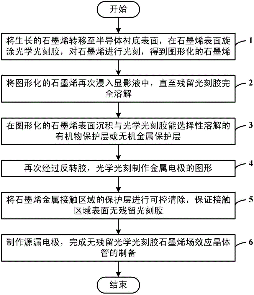
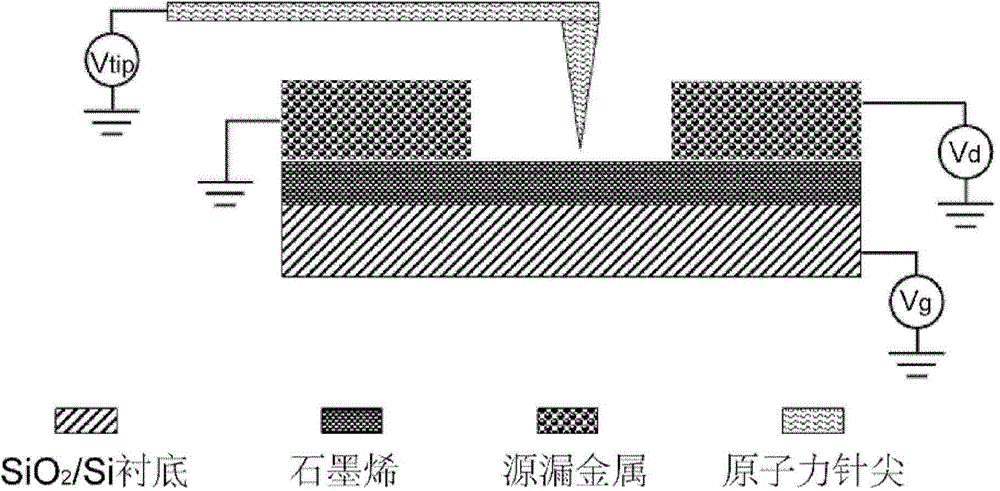
[0054] based on figure 1 The flow chart of the method for preparing no-residue optical photoresist graphene field-effect transistor shown, figure 2 shows that in accordance with figure 1 Schematic diagram of in-situ characterization of the prepared residue-free graphene field-effect transistor, the in-situ characterization method includes:

[0055] Step 1: Using EFM or conductive AFM to characterize and study the change of carrier mobility in graphene in the device within the range of the applied electric field on a microscopic scale; wherein, the change range of the applied electric field is -3~+3V.

[0056] Step 2: On the basis of EFM or conductive AFM characterization, use the tip of AFM as a test probe, use the oxide layer of the substrate itself as a medium, and monitor the gate control characteristics of graphene in real time for in-situ characterization; among them, the substrate The Si substrate is selected, and the oxide layer of the substrate itself is SiO with a ...

Embodiment 1

[0060] The preparation method of the graphene FET without residual optical photoresist comprises the following steps, specifically comprising:

[0061] 1) Transfer the single-layer uniform graphene grown on the surface of copper foil by CVD to SiO with a 330nm insulating layer 2 / Si substrate surface. Spin-coat a layer of 9912 positive photoresist with a thickness of 1.4 μm on the surface of the substrate spread with graphene, after exposure (light intensity 5, time 15 seconds), development (40 seconds), primer, and acetone to remove the glue , patterning the active region of graphene;

[0062] 2) Immerse the patterned graphene in the positive resist developer again, let it stand for 10 seconds, and dry it with nitrogen;

[0063] 3) On the patterned graphene surface, deposit 10nm metal nickel as a protective layer of graphene by electron beam evaporation technology;

[0064] 4) Spin-coat a layer of AZ5214 reverse glue with a thickness of 1.4 μm on the surface of the protect...

Embodiment 2

[0073] The preparation scheme of graphene FET without residual optical photoresist includes the following steps, specifically including:

[0074] 1) A single layer of uniform graphene grown on the surface of copper foil by CVD is transferred to SiO with a 300nm insulating layer 2 / Si substrate surface. Spin-coat a layer of 9920 positive photoresist with a thickness of 1.4 μm on the surface of the substrate spread with graphene, after exposure (light intensity 5, time 15 seconds), development (40 seconds), Matrix primer, acetone to remove Glue to pattern the active area of ​​graphene;

[0075] 2) Immerse the patterned graphene in the positive resist developer again, let it stand for 10 seconds, and dry it with nitrogen;

[0076] 3) on the patterned graphene surface, adopt the method for spin-coating to deposit 20nm α-methyl polystyrene as the protective layer of graphene;

[0077] 4) Spin-coat a layer of AZ5214 reverse glue with a thickness of 1.4 μm on the surface of the pr...


PUM

PropertyMeasurementUnit
thicknessaaaaaaaaaa
thicknessaaaaaaaaaa
thicknessaaaaaaaaaa

Abstract

The invention discloses a manufacturing method and an in-situ characterizing method for a graphene field effect transistor free of residual optical photoresist. The manufacturing method includes the following steps that growing graphene is transferred to the surface of a semiconductor substrate, the surface of the graphene is coated with optical photoresist in a spinning mode, photoetching is conducted on the graphene, and patterned graphene is obtained; the patterned graphene is immersed into a developing solution again until the residual optical photoresist is dissolved completely; an organic matter protecting layer or an inorganic metal protecting layer capable of being selectively dissolved with the optical photoresist is deposited on the surface of the patterned graphene; patterns of a metal electrode are made again through inversion photoresist in an optical lithography mode; the protecting layer of the graphene-metal contact region is cleared away controllably, and it is guaranteed that no photoresist remains on the surface of the contact region; source and drain electrodes are made, and manufacturing of the graphene field effect transistor free of the residual optical photoresist is completed. Influences of the residual optical photoresist on the carrier mobility of the graphene are characterized by means of the technologies such as atomic force microscopy and electrostatic force microscopy.

Description

technical field [0001] The invention relates to the technical field of field effect transistor preparation, in particular to a preparation method of a graphene field effect transistor (FET) without residual optical photoresist and an in-situ characterization method of a graphene FET without residual optical photoresist. Background technique [0002] With the development of microelectronics technology, various effects appearing at small sizes make the continuation of Moore's Law difficult, silicon-based microelectronics technology is gradually approaching its theoretical limit, and carbon-based materials have shown special characteristics in nanoelectronics technology. The advantages. Among them, graphene is a new type of material that has attracted wide attention in recent years. Its excellent physical and electrical properties make graphene materials have broad application prospects in the new generation of high-performance microelectronics and circuits, especially in ultra...

Claims


Application Information

Patent Timeline
Patent Type & Authority Applications(China)
IPC IPC(8): H01L21/336H01L21/027H01L21/66
Inventor 金智彭松昂史敬元王少青王选芸张大勇
Owner INST OF MICROELECTRONICS CHINESE ACAD OF SCI
Why Eureka
Try Eureka