

Crystalline silicon solar cell and preparation method thereof
A technology of solar cells and crystalline silicon, applied in the field of solar energy, can solve the problems of unavailable industrial production and low photoelectric conversion efficiency of cells, and achieve the effects of improving photoelectric conversion efficiency, strong practicability, and mature equipment technology
- Summary
- Abstract
- Description
- Claims
- Application Information
AI Technical Summary
Problems solved by technology
Method used
Image

Examples
preparation example Construction
[0023] The present invention also provides a preparation method for the crystalline silicon solar cell, comprising the following steps:
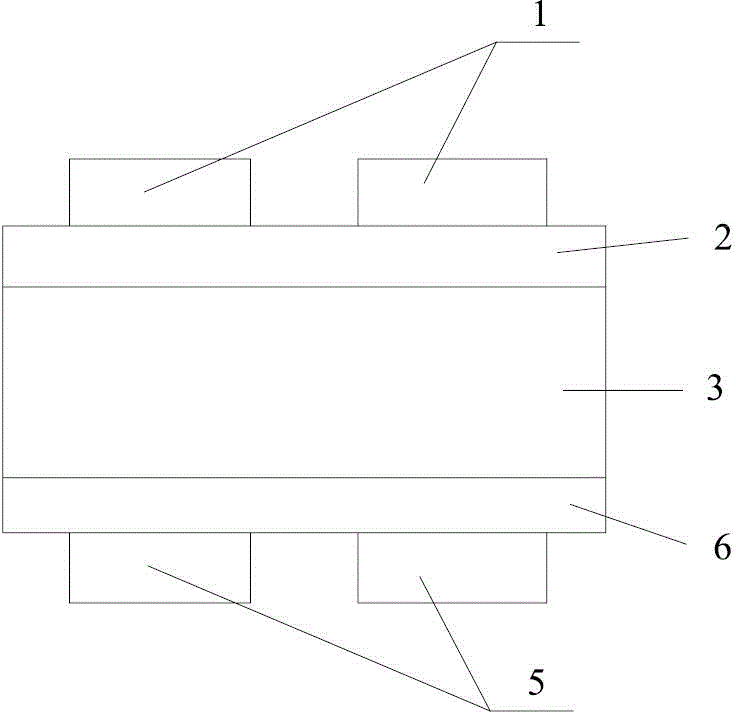
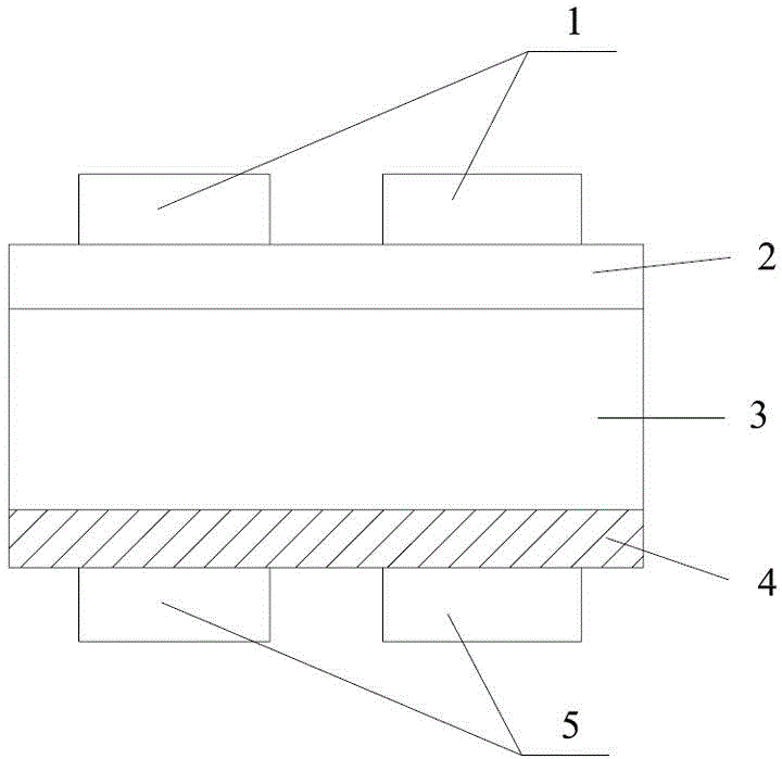
[0024] S10, performing texturing, diffusion and wet etching on the surface of the silicon substrate, and then coating an anti-reflection film on one surface of the silicon substrate, and polishing the other surface;
[0025] S20. Place the silicon substrate that has passed step S10 in a vacuum coating chamber, and coat a passivation layer on its polished surface by vacuum coating; the target material of the vacuum coating is a metal-doped silicon oxide target, doped The metal is aluminum and / or tin, and the vacuum coating atmosphere contains hydrogen or ammonia;
[0026] S30, forming a back electrode layer on the surface of the passivation layer, and forming a front electrode layer on the surface of the antireflection film, to obtain the crystalline silicon solar cell.
[0027] The preparation method of the crystalline silicon solar cell pr...
Embodiment 1
[0043] (1) A crystalline silicon wafer treated with texturing / diffusion / wet etching / plasma-enhanced chemical vapor deposition (PECVD) and coated with silicon nitride was taken as the silicon substrate of this embodiment, and its size was 156×156 mm, and its The silicon nitride anti-reflection film attached to the surface has a thickness of 120nm. Then chemical polishing is used to polish the silicon surface not coated with silicon nitride anti-reflection film.
[0044] (2) Send the above-mentioned silicon wafer into the preheating chamber, and preheat at 250°C for 20 minutes with an infrared lamp. Send the preheated silicon wafer into the coating chamber, vacuumize the coating chamber first and then fill it with reaction gas until the vacuum degree is 2×10 -3 Pa, when the temperature is 200°C, clean the silicon wafer for 10 minutes, and then perform a pre-sputtering operation on the target. The coating target is silicon oxide doped with aluminum (the aluminum content in the t...
Embodiment 2
[0047] (1) A crystalline silicon wafer treated with texturing / diffusion / wet etching / plasma-enhanced chemical vapor deposition (PECVD) and coated with silicon nitride was taken as the silicon substrate of this embodiment, and its size was 156×156 mm, and its The silicon nitride anti-reflection film attached to the surface has a thickness of 120nm. Then chemical polishing is used to polish the silicon surface not coated with silicon nitride anti-reflection film.
[0048] (2) Send the above-mentioned silicon wafer into the preheating chamber, and preheat at 250°C for 20 minutes with an infrared lamp. Send the preheated silicon wafer into the coating chamber, vacuumize the coating chamber first and then fill it with reaction gas until the vacuum degree is 2×10 -3 Pa, when the temperature is 200°C, clean the silicon wafer for 10 minutes, and then perform a pre-evaporation operation on the target material. The coating target material is silicon oxide doped with aluminum (the alumin...
PUM
| Property | Measurement | Unit |
|---|---|---|
| Thickness | aaaaa | aaaaa |
| Thickness | aaaaa | aaaaa |
| Thickness | aaaaa | aaaaa |
Abstract
Description
Claims
Application Information