Resonance tunneling diode with double InGaN sub quantum wells and manufacturing method thereof

A resonant tunneling and diode technology, applied in the direction of electrical components, circuits, semiconductor devices, etc., can solve the problems of high activation energy and defect density, device I-V characteristic attenuation, high interface roughness, etc., to reduce dislocation density and activation performance, lower threshold voltage, and lower power consumption

Active Publication Date: 2015-03-25
晋江三伍微电子有限公司
View PDF5 Cites 13 Cited by
  • Summary
  • Abstract
  • Description
  • Claims
  • Application Information

AI Technical Summary

Problems solved by technology

However, due to the high lattice mismatch, high interface roughness and strong piezoelectric polarization at the AlGaN / GaN heterojunction interface, the activation energy and defect density of the trap centers at the interface are too large, and the I-V characteristics of the device under multiple scans Severe attenuation

Method used


Image

  • Resonance tunneling diode with double InGaN sub quantum wells and manufacturing method thereof
  • Resonance tunneling diode with double InGaN sub quantum wells and manufacturing method thereof
  • Resonance tunneling diode with double InGaN sub quantum wells and manufacturing method thereof

Examples


Embodiment 1

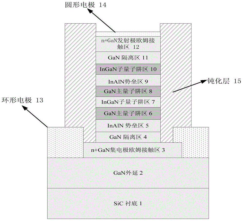
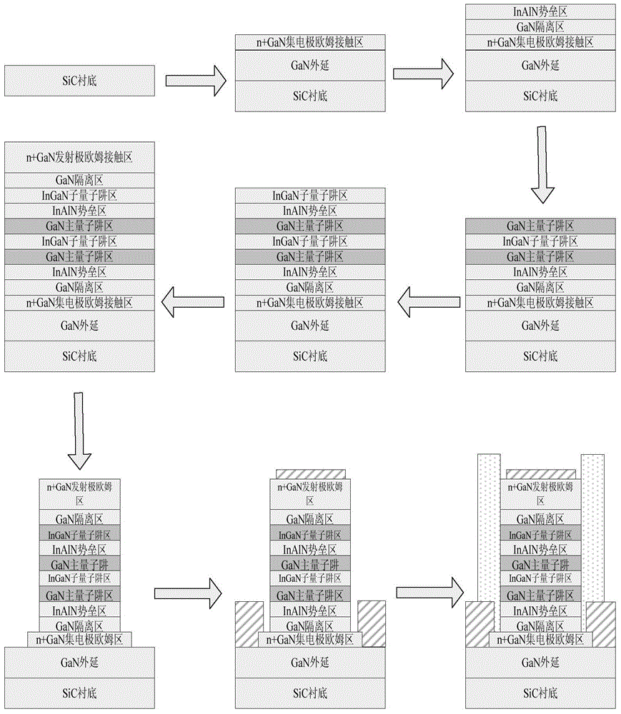
[0040] Embodiment 1: Fabricate a resonant tunneling diode with a first InGaN sub-quantum well layer with a thickness of 0.8nm and an In composition of 3% and a second InGaN sub-quantum well layer with a thickness of 0.8nm and an In composition of 3%.

[0041] In step 1, a SiC substrate is selected.

[0042] A 4H-SiC insulating SiC substrate with a diameter of 2 inches is selected, and the back side thereof is thinned to a thickness of 150 μm.

[0043] Step 2, epitaxial GaN layer on SiC substrate.

[0044] Using triethylgallium and high-purity nitrogen as the source of gallium and nitrogen respectively, under the conditions of temperature 450 ℃ and pressure 40 torr, metal-organic chemical vapor deposition MOCVD method was used to epitaxially grow thickness 2 μm GaN layer.

[0045] Step 3, grow n on the GaN epitaxial layer + GaN collector ohmic contact layer.

[0046] Using triethylgallium and high-purity nitrogen as the gallium source and nitrogen source respectively, using...

Embodiment 2

[0084] Embodiment 2: Fabricate a resonant tunneling diode with a first InGaN sub-quantum well layer with a thickness of 1 nm and an In composition of 5% and a second InGaN sub-quantum well layer with a thickness of 1 nm and an In composition of 5%.

[0085] Step 1: Select a 6H-SiC insulating SiC substrate with a diameter of 2 inches, and thin the back surface to a substrate thickness of 150 μm.

[0086] Step 2, using triethylgallium and high-purity nitrogen as the gallium source and nitrogen source respectively, using metal organic chemical vapor deposition MOCVD method, under the process conditions of temperature of 450 °C and external pressure of 40 Torr, the epitaxial growth thickness is 2μm GaN layer.

[0087] Step 3, using high-purity nitrogen gas and triethylgallium as the nitrogen source and gallium source respectively, and silane gas as the n-type doping source, using metal organic chemical vapor deposition MOCVD method, at a temperature of 1000 ° C and a pressure of 4...

Embodiment 3

[0104] Embodiment 3: Fabricate a resonant tunneling diode with a first InGaN sub-quantum well layer with a thickness of 1.2nm and an In composition of 7% and a second InGaN sub-quantum well layer with a thickness of 1.2nm and an In composition of 7%.

[0105] Step A, select a 6H-SiC conduction-type n-type SiC substrate with a diameter of 2 inches, and a doping concentration of 2.0×10 18 cm -3 , the backside is thinned to a substrate thickness of 150 μm.

[0106] Step B, epitaxially growing a GaN layer, n + GaN collector ohmic contact layer and GaN isolation layer:

[0107] (B1) Using triethylgallium and high-purity nitrogen as gallium source and nitrogen source, using metal organic chemical vapor deposition MOCVD method, under the process conditions of temperature 450 ℃ and pressure 40 torr, epitaxial growth on the substrate GaN layer with a thickness of 3 μm;

[0108] (B2) using the same nitrogen source and gallium source as in (B1), using silane gas as the n-type doping ...


PUM


Abstract

The invention discloses a resonance tunneling diode with double InGaN sub quantum wells. The resonance tunneling diode mainly solves the problems that an existing device is small in tunneling current and poor in I-V character repeatability. The resonance tunneling diode comprises a main body and an auxiliary body, the main body is divided into a SiC substrate layer, a GaN epitaxial layer, an n+GaN collector ohmic contact layer, a first GaN isolating layer, a first InAlN barrier layer, a first GaN main quantum well layer, a second GaN main quantum layer, a second InAlN barrier layer, a second GaN isolating layer and an n+GaN emitter diode ohmic contact layer from bottom to top, and the auxiliary part is provided with an annular electrode, a round electrode and a passivation layer. The annular electrode is arranged above the n-GaN collector ohmic contact layer, the round electrode is arranged above the n+GaN emitter ohmic contact layer, and the passivation layer is arranged above the annular electrode and the round electrode. The resonance tunneling diode can effectively improve the power of the device, reduce power consumption and improve the repeatability and is suitable for the terahertz radiation frequency band work.

Description

technical field [0001] The invention belongs to the technical field of microelectronic devices, and relates to a resonant tunneling diode of a wide bandgap semiconductor GaN material and a manufacturing method, which can be used for manufacturing high-frequency and high-power devices. Background technique [0002] In recent years, the third-generation wide-bandgap semiconductor materials represented by gallium nitride GaN and silicon carbide SiC follow the first-generation semiconductor materials represented by semiconductor Si and the second-generation semiconductor materials represented by GaAs. A new type of semiconductor material that has developed rapidly in the past ten years. GaN-based semiconductor materials and devices are subject to great influence due to their excellent characteristics such as large bandgap width, high conduction band discontinuity, high thermal conductivity, high critical field strength, high carrier saturation rate, and high two-dimensional elec...

Claims


Application Information

Patent Timeline
Patent Type & Authority Applications(China)
IPC IPC(8): H01L33/06H01L33/32
CPCH01L33/0075H01L33/06H01L33/32H01L2933/0008H01L2933/0066
Inventor 杨林安陈浩然李月田言陈安郝跃
Owner 晋江三伍微电子有限公司
Why Eureka
Try Eureka