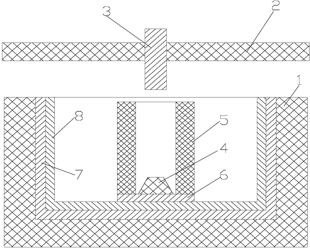
Material for filter chamber and filter chamber
A filter and cavity technology, used in waveguide-type devices, electrical components, circuits, etc., can solve problems such as unfavorable heat dissipation and low thermal conductivity, and achieve the effect of solving inconsistent thermal expansion coefficients, high thermal conductivity, and high thermal conductivity.
- Summary
- Abstract
- Description
- Claims
- Application Information
AI Technical Summary
Problems solved by technology
Method used
Image
Examples
Embodiment 1
[0036] The material used for the filter cavity in this embodiment is a composite material formed by adding metal aluminum to silicon carbide—aluminum silicon carbide, the amount of metal aluminum added accounts for 37% of the total volume of aluminum silicon carbide by volume, and the formation method is The SiC green body is formed by cold isostatic pressing process, formed after aluminizing at high temperature, and the filter cavity is formed by wire cutting, which can also be formed by laser cutting;
[0037] As shown in the figure, the inner surface of the filter cavity of this embodiment is plated with a 4 μm copper conductive layer, and the surface of the copper conductive layer is electroplated or deposited to form a 4 μm silver conductive layer; of course, gold can be used instead of silver, and the thickness can be reduced , generally choosing a thickness not less than 2 μm can also achieve the purpose of the invention.
[0038]In this embodiment, the bottom of the fi...
Embodiment 2
[0042] The material used for the filter cavity in this embodiment is a composite material formed by adding metal aluminum to silicon carbide—aluminum silicon carbide, the amount of metal aluminum added accounts for 45% of the total volume of aluminum silicon carbide by volume, and the formation method is It is formed by metallurgy of SiC and metal aluminum powder and fired at high temperature, and the filter cavity is formed by wire cutting, and can also be formed by laser cutting;
[0043] As shown in the figure, the inner surface of the filter cavity of this embodiment is plated with a 6 μm copper conductive layer, and a 4 μm silver conductive layer is formed on the surface of the copper conductive layer by electroplating or deposition; of course, gold can be used instead of silver, and the thickness can be reduced , generally choosing a thickness not less than 2 μm can also achieve the purpose of the invention.
[0044] In this embodiment, the bottom of the filter cavity is...
Embodiment 3
[0047] The material used for the filter cavity in this embodiment is a composite material formed by adding metal aluminum to silicon carbide—aluminum silicon carbide, the amount of metal aluminum added accounts for 63% of the total volume of aluminum silicon carbide by volume, and the formation method is The SiC green body is formed by gel-injection molding net size forming process, formed after aluminizing at high temperature, and the filter cavity is formed by wire cutting processing, which can also be formed by laser cutting;
[0048] As shown in the figure, the inner surface of the filter cavity of this embodiment is plated with a 12 μm copper conductive layer, and the surface of the copper conductive layer is electroplated or deposited to form a 2 μm gold conductive layer; of course, silver can be used instead of gold, and the thickness can be increased appropriately , generally choosing a thickness not less than 4 μm can also achieve the purpose of the invention.
[0049...
PUM
| Property | Measurement | Unit |
|---|---|---|
| thickness | aaaaa | aaaaa |
| thickness | aaaaa | aaaaa |
| flexural strength | aaaaa | aaaaa |
Abstract
Description
Claims
Application Information
 - R&D
- Intellectual Property
- Life Sciences
- Materials
- Tech Scout
- Unparalleled Data Quality
- Higher Quality Content
- 60% Fewer Hallucinations
Browse by: Latest US Patents, China's latest patents, Technical Efficacy Thesaurus, Application Domain, Technology Topic, Popular Technical Reports.
© 2025 PatSnap. All rights reserved.Legal|Privacy policy|Modern Slavery Act Transparency Statement|Sitemap|About US| Contact US: help@patsnap.com

