

Preparation method of film material for compound semiconductor
A technology of thin film materials and semiconductors, applied in the field of thin film material manufacturing, to achieve the effects of good crystallinity, low preparation temperature and simple preparation equipment
- Summary
- Abstract
- Description
- Claims
- Application Information
AI Technical Summary
Problems solved by technology
Method used
Image

Examples
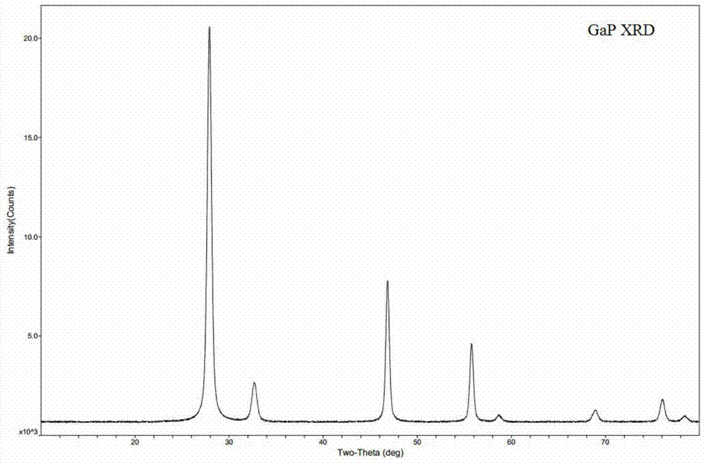
Embodiment 1
[0070] Method and process for preparing GaP by two-step method
[0071] The method for preparing GaP thin film material, comprises the following steps:
[0072] Step 1. Accurately weigh Ga with a ten-thousandth electronic analytical balance 2 o 3 , P 2 o 5 , according to the molar ratio Ga / P=1.0 / 1.0, mix and grind evenly, add anhydrous ethanol equivalent to 50% of the solid raw material mass, grind again carefully, remove the solvent by drying, and press it into a thickness with a pressure of 12MPa Then seal it in a vacuum ampoule, place the ampoule in the corundum crucible of the reactor, heat it to 500°C in a tube electric furnace, keep the temperature for 2h, and get GaPO after natural cooling. 4 Solid material, confirmed by XRD diffraction analysis results;
[0073] Step 2. Break the ampoule and place GaPO 4 In the reaction zone of the vertical gradient condensation thin film deposition device, the substrate is placed at the designated position in the deposition area...
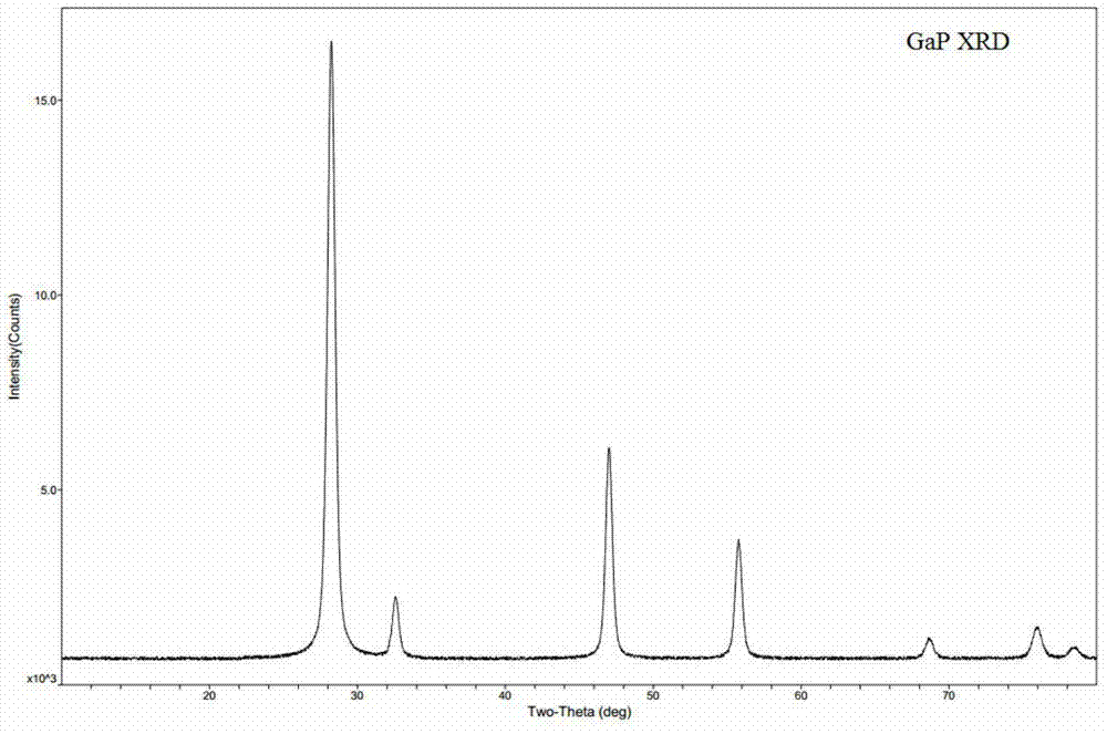
Embodiment 2
[0076] Method and process for preparing GaP by one-step method
[0077] Accurately Weighing Ga with 1 / 10000 Electronic Analytical Balance 2 o 3 , P 2 o 5 , activated carbon C, uniformly mixed and ground according to the ratio of molar ratio Ga:P:C=1.0:1.0:8.0, adding anhydrous ethanol equivalent to 50% of the solid raw material mass, carefully grinding it evenly, and pressing it with a pressure of 10MPa A disc with a thickness of 1mm is then placed in the corundum crucible of the reactor, vacuumed and replaced with high-purity nitrogen to an oxygen concentration above the ppm level, and then Ar+H 2 Mixed gas (including H 2 The volume percentage is 10%) and replaced once by vacuuming. After the substrate required for deposition is processed, it is pre-placed in the designated position in the reactor, and then vacuumed to about 1mmHg. The heating rate is controlled at 5°C / min, and the heating is started until the reaction Zone 1200°C, deposition zone 600°C, turn on the subs...
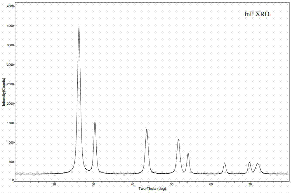
Embodiment 3
[0080] Method and process for preparing InP by two-step method
[0081] The method for preparing GaP thin film material, comprises the following steps:
[0082] Step 1. Accurately weigh In with a ten-thousandth electronic analytical balance 2 o 3 , P 2 o 5 , according to the molar ratio In: P = 1.0: 1.0 ~ 1.5, mix and grind evenly, add anhydrous ethanol equivalent to 50% ~ 100% of the solid raw material quality, grind again carefully, remove the solvent by drying, and use 10 ~ 15MPa Press it into a disc with a thickness of 3mm, then seal it in a vacuum ampoule, place the ampoule in the corundum crucible of the reactor, and heat it to 500°C to 600°C in a self-made tube electric furnace. Constant temperature for 2 to 4 hours, natural cooling, that is, InPO 4 solid material;
[0083] Step 2. Break the ampoule, put the InPO 4 The solid material is placed in the reaction zone of the vertical gradient condensation thin film deposition device, and replaced with high-purity nit...
PUM
| Property | Measurement | Unit |
|---|---|---|
| thickness | aaaaa | aaaaa |
| lattice constant | aaaaa | aaaaa |
| melting point | aaaaa | aaaaa |
Abstract
Description
Claims
Application Information