Organic light-emitting device and preparation method thereof
An electroluminescent device and luminescence technology, which is applied in the fields of electric solid-state devices, semiconductor/solid-state device manufacturing, electrical components, etc., can solve problems such as short service life, poor mechanical strength, and complicated preparation process
- Summary
- Abstract
- Description
- Claims
- Application Information
AI Technical Summary
Problems solved by technology
Method used
Image

Examples
Embodiment 1
[0082] An organic electroluminescent device is prepared through the following steps:
[0083] (1) Provide a clean anode conductive substrate:
[0084] Clean the ITO glass substrate with acetone, ethanol, deionized water, and ethanol in an ultrasonic cleaner in sequence, wash and wash for 5 minutes in one item, then blow dry with nitrogen, and dry in an oven for later use; surface activation of the cleaned ITO glass processing; ITO thickness is 100nm;
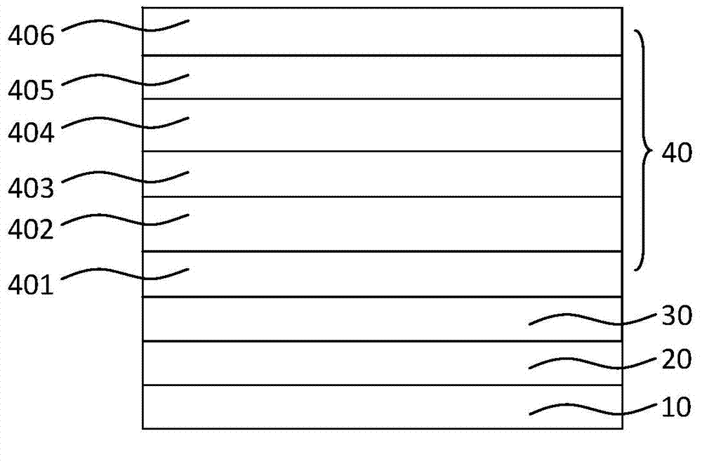
[0085] (2) Vacuum evaporation of the luminescent functional layer on the ITO glass substrate:
[0086] Specifically, the light emitting functional layer includes a hole injection layer, a hole transport layer, a light emitting layer, an electron transport layer and an electron injection layer;
[0087] Preparation of the hole injection layer: the MoO 3 The mixture obtained by mixing with NPB according to the mass ratio of 1:3 is used as the material of the hole injection layer, the thickness is 10nm, and the vacuum degree is ...
Embodiment 2
[0105] An organic electroluminescent device is prepared through the following steps:
[0106] (1), (2), (3) are the same as embodiment 1;
[0107] (4) Prepare the encapsulation layer on the outside of the cathode:
[0108] The encapsulation layer is alternately stacked silicon oxynitride barrier layers and inorganic barrier layers;
[0109] Fabrication of silicon oxynitride barrier layer: HMDS, NH 3 , O 2 As the source, argon gas was introduced, and a silicon oxynitride film was prepared in a PECVD deposition chamber to obtain a silicon oxynitride barrier layer. The preparation process conditions were HMDS flow rate 14 sccm, NH 3 Flow 18sccm, O 2 The flow rate is 18sccm, the flow rate of argon gas is 80sccm, and the thickness of the silicon oxynitride film is 190nm;
[0110] Fabrication of the inorganic barrier layer: the organic electroluminescent device sample prepared with the silicon oxynitride barrier layer was placed in the deposition chamber of the atomic layer dep...
Embodiment 3
[0116] An organic electroluminescent device is prepared through the following steps:
[0117] (1), (2), (3) are the same as embodiment 1;
[0118] (4) Prepare the encapsulation layer on the outside of the cathode:
[0119] The encapsulation layer is alternately stacked silicon oxynitride barrier layers and inorganic barrier layers;
[0120] Fabrication of silicon oxynitride barrier layer: HMDS, NH 3 , O 2 As the source, argon gas was introduced to prepare a silicon oxynitride film in a PECVD deposition chamber to obtain a silicon oxynitride barrier layer. The preparation process conditions were HMDS flow rate 12 sccm, NH 3 Flow 15sccm, O 2 The flow rate is 16sccm, the flow rate of argon gas is 76sccm, and the thickness of the silicon oxynitride film is 180nm;
[0121] Fabrication of the inorganic barrier layer: the organic electroluminescent device sample prepared with the silicon oxynitride barrier layer was placed in the deposition chamber of the atomic layer deposition...
PUM
| Property | Measurement | Unit |
|---|---|---|
| Thickness | aaaaa | aaaaa |
| Thickness | aaaaa | aaaaa |
| Thickness | aaaaa | aaaaa |
Abstract
Description
Claims
Application Information
 - R&D
- Intellectual Property
- Life Sciences
- Materials
- Tech Scout
- Unparalleled Data Quality
- Higher Quality Content
- 60% Fewer Hallucinations
Browse by: Latest US Patents, China's latest patents, Technical Efficacy Thesaurus, Application Domain, Technology Topic, Popular Technical Reports.
© 2025 PatSnap. All rights reserved.Legal|Privacy policy|Modern Slavery Act Transparency Statement|Sitemap|About US| Contact US: help@patsnap.com