Graphene/cadmium telluride solar battery intensified by cadmium selenide and preparation method thereof
A technology of solar cells and cadmium selenide, which is applied in the field of solar cells, can solve the problems of narrow band gap of silicon materials and not being a basic material, and achieve the effects of low cost, simple preparation process, and improved photoelectric conversion efficiency
- Summary
- Abstract
- Description
- Claims
- Application Information
AI Technical Summary
Problems solved by technology
Method used
Image

Examples
Embodiment 1
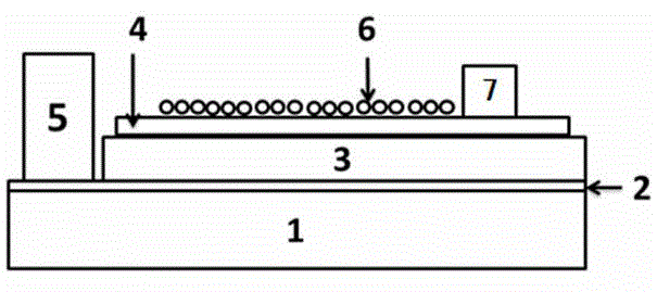
[0024] 2) Deposit 40 nm thick indium-doped tin oxide on polyimide flexible substrate by magnetron sputtering;
[0025] 3) Deposit a cadmium telluride layer with a thickness of 6 microns on the indium-doped tin oxide layer by physical vapor deposition technology, and reserve an area for growing the first electrode on the ITO layer;
[0026] 4) Transfer single-layer graphene onto the cadmium telluride layer;
[0027] 5) Spin-coat the cadmium selenide quantum dot solution on the graphene, and reserve an area for growing the second electrode on the graphene; the diameter of the cadmium selenide quantum dot is 1nm-1μm;
[0028] 6) Coating silver paste on the reserved area of the graphene and the reserved area on the ITO layer and drying; a graphene / cadmium telluride solar cell enhanced by cadmium selenide is obtained.
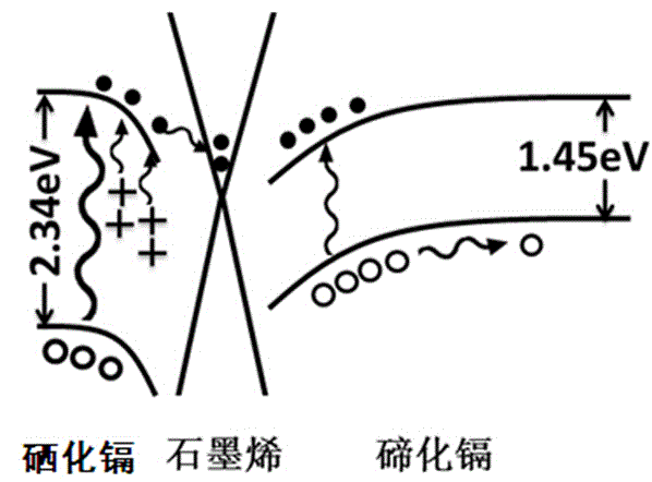
[0029] The energy band structure diagram of the graphene / cadmium telluride solar cell enhanced by cadmium selenide obtained is attached figure 2 As shown, the ...
Embodiment 2
[0032] 2) Deposit 200 nm thick fluorine-doped tin oxide on a glass substrate by magnetron sputtering;
[0033] 3) Deposit an 8-micron-thick cadmium telluride layer on the fluorine-doped tin oxide layer using physical vapor deposition technology, and reserve an area for growing the first electrode on the FTO layer;
[0034] 4) Transfer three layers of graphene onto the cadmium telluride layer;
[0035] 5) Spraying the cadmium selenide quantum dot solution on the graphene, and reserve the area for growing the second electrode on the graphene layer; the diameter of the cadmium selenide quantum dot is 1nm-1μm;
[0036] 6) Thermally evaporate gold electrodes on the reserved area of the graphene layer and the reserved area on the fluorine-doped tin oxide layer; obtain a graphene / cadmium telluride solar cell enhanced by cadmium selenide.
[0037] Example 3:
Embodiment 3
[0039] 2) Deposit 60nm-thick nickel metal on a ceramic substrate by electron beam evaporation;
[0040] 3) Deposit a cadmium telluride layer with a thickness of 5 microns on the nickel metal layer by chemical water bath method, and reserve an area for growing the first electrode on the nickel metal layer;
[0041] 4) Transfer 10 layers of graphene onto the cadmium telluride layer;
[0042] 5) Prepare a cadmium selenide film on graphene, and reserve an area for growing the second electrode on the graphene layer;
[0043] 6) Silver electrodes are screen-printed on the reserved area of the graphene layer and the reserved area on the nickel metal layer; a cadmium selenide-enhanced graphene / cadmium telluride solar cell is obtained.
[0044] Example 4:
PUM
| Property | Measurement | Unit |
|---|---|---|
| diameter | aaaaa | aaaaa |
Abstract
Description
Claims
Application Information