
Method for treating ILD (injection laser diode) layer in gate-last technology

A processing method and gate-last process technology, applied to semiconductor devices, electrical components, circuits, etc., can solve problems such as small process windows, affecting device performance, and difficulty in control, so as to reduce the difficulty of device integration, improve the process window, and improve the cost efficiency. effect of density

Inactive Publication Date: 2015-05-20
INST OF MICROELECTRONICS CHINESE ACAD OF SCI
View PDF10 Cites 3 Cited by
  • Summary
  • Abstract
  • Description
  • Claims
  • Application Information

AI Technical Summary

Problems solved by technology

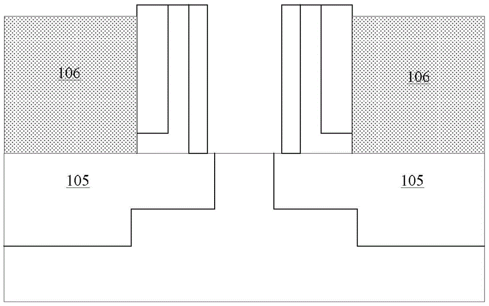
[0003] In the usual gate-last process, after forming the dummy gate structure and the ILD layer, CMP is first performed until the dummy gate is exposed, then the dummy gate and the dummy gate dielectric layer are removed, and then the gate dielectric layer is re-formed. The dummy gate dielectric layer is usually Thermal oxide formation, ILD is mostly an oxide layer formed by CVD (Chemical Vapor Deposition, chemical vapor deposition) and other methods, dHF (diluted HF, diluted hydrofluoric acid) or dBOE (diluted HF) is usually used to remove the dummy gate dielectric layer Buffered Oxide Etch, diluted buffer solution), due to the different preparation methods, the density of the dummy gate dielectric layer and the ILD is also different, that is, the ILD has a faster etching rate, which will cause the loss of the ILD layer 106, such as figure 2 As shown, in this process, the removal of CMP and the dummy gate dielectric layer will cause the loss of ILD. The loss of ILD will affect the height of the re-formed replacement gate and reduce the normal performance of the device. If it is not handled properly, the device may even fail to work.
Since the process window of CMP is very small and difficult to control, in the actual process, the height of the dummy gate is often used to make up for the loss of ILD, but with the continuous reduction of process size, this method cannot solve the problem of ILD loss question
Especially in Fin-FET (Fin Field Effect Transistor) 3D devices, because there is no silicon nitride layer on the top of the device fin, CMP control is more difficult, and in order to obtain the ideal shape of the fin, a thicker dummy gate is usually formed Dielectric layer, which will inevitably increase the time to remove the dummy gate dielectric layer, which will cause more obvious ILD loss, and then it is difficult to obtain the ideal gate height, affecting the performance of the device

Method used


Image

  • Method for treating ILD (injection laser diode) layer in gate-last technology
  • Method for treating ILD (injection laser diode) layer in gate-last technology
  • Method for treating ILD (injection laser diode) layer in gate-last technology

Examples


Embodiment 1

[0028] The invention mainly aims at the loss of the ILD layer in the process of removing the dummy gate dielectric layer in the gate-last process. Generally, in the gate-last process, before forming the ILD layer, it mainly includes the following step S101 of forming a dummy gate device:

[0029] provide the substrate;

[0030] sequentially forming a dummy gate dielectric layer and a dummy gate on the substrate;

[0031] A spacer is formed on the sidewall of the dummy gate, and a source drain is formed on both sides of the dummy gate.

[0032] In the embodiment of the present invention, refer to Figure 4 As shown, the semiconductor substrate 200 may be a Si substrate, a Ge substrate, a Si-Ge substrate, SOI (Silicon On Insulator, Silicon On Insulator) or GOI (Germanium On Insulator, Germanium On Insulator) and the like. In other embodiments, the semiconductor substrate may also be a substrate including other elemental semiconductors or compound semiconductors, such as GaAs,...

Embodiment 2

[0047] The formation method of the first embodiment of the present invention has been described in detail above. In the second embodiment, the difference from the first embodiment is that after the CMP of the ILD, the nitriding treatment is performed first, and then the thermal annealing is performed, thereby improving the ILD. corrosion resistance. Only the differences will be described below, and other similarities with Embodiment 1 will not be repeated.

[0048] In step S201, a dummy gate device is formed, which is the same as step S101 in the first embodiment.

[0049] Then, in step S202 , the source and drain regions are covered, and further chemical polishing is performed to form an ILD (Inter Layer Dielectric) layer, which is the same as step S102 in the first embodiment.

[0050] Then, in step S2021, nitriding treatment is performed.

[0051] In this embodiment, DPN (decoupled plasma nitriding, decoupled plasma nitriding) is used for nitriding treatment, so that the ...


PUM


Abstract

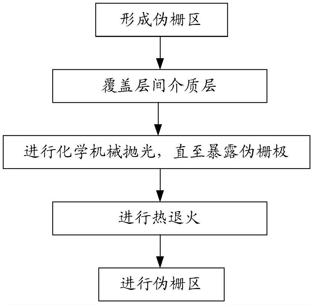
The invention provides a method for treating an ILD (injection laser diode) layer in a gate-last technology. The method comprises the following steps of forming a pseudo gate region; covering an interlayer dielectric layer; performing chemico-mechanical polishing until a pseudo gate electrode is exposed; performing thermal annealing; and removing the pseudo gate region. Thermal annealing is carried out after the ILD layer is formed, the density of the ILD layer can be improved by a thermal annealing process, and the etching rate of the ILD layer can be reduced when the pseudo gate dielectric layer is removed, so that loss of the ILD layer is reduced.

Description

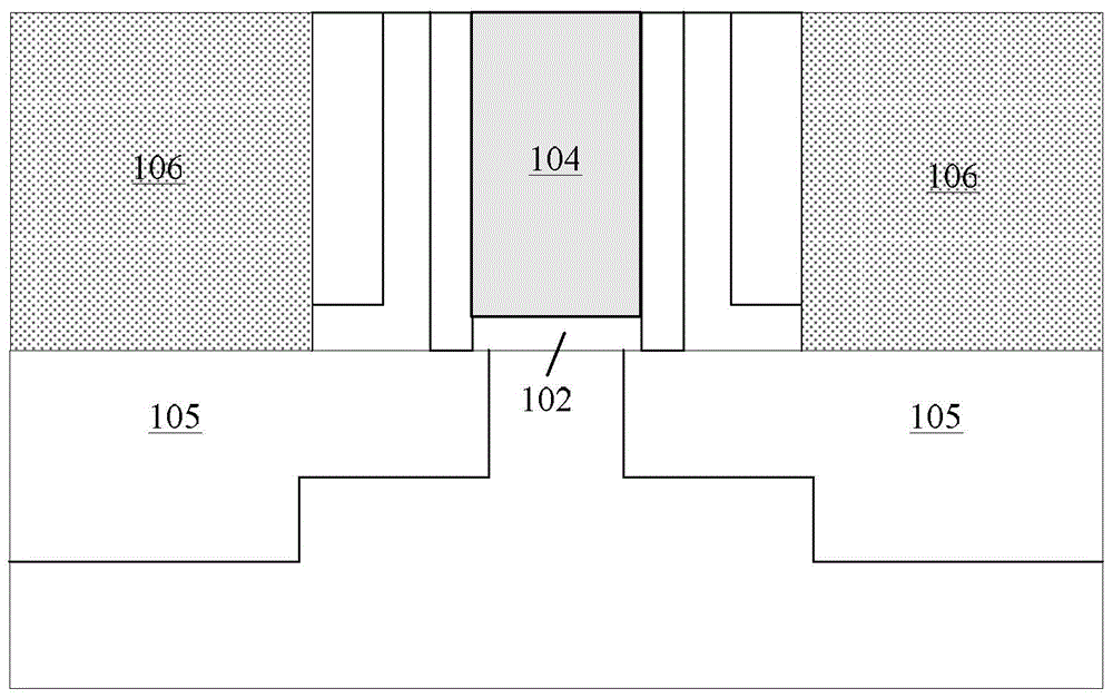
technical field [0001] The invention relates to the field of semiconductor manufacturing, in particular to a method for processing an ILD layer in a gate-last process. Background technique [0002] At present, the research on the manufacturing process of CMOSFET (Complementary Metal Oxide Semiconductor Field Effect Transistor) can be roughly divided into two directions, namely, the front gate process and the gate replacement process. Previously, all high-temperature annealing processes limited and could negatively impact gate layer material selection. The gate replacement process (gate last process, Gate Last), such as figure 1 As shown, the dummy gate 104, the dummy gate dielectric layer 102, the source and drain electrodes 105, and the ILD (interlayer dielectric) layer 106 are first formed, and then the dummy gate 104 is removed to form the gate again. In this way, the gate is formed after the source and drain, In this process, the gate does not need to withstand a high ...

Claims


Application Information

Patent Timeline
IPC IPC(8): H01L21/28
CPCH01L21/28H01L21/324
Inventor 崔虎山熊文娟殷华湘罗军张永奎徐强朱慧珑赵超
Owner INST OF MICROELECTRONICS CHINESE ACAD OF SCI
Learn More