Hybrid membrane production method

A hybrid film, compound technology, applied in semiconductor/solid state device manufacturing, nanotechnology for materials and surface science, electrical components, etc., can solve the problem of poor repeatability of hybrid materials, limiting composite film mobility, polymer Poor stability and other problems, to achieve the effect of easy large-scale mass production, low cost, and short production cycle

Inactive Publication Date: 2015-06-10
SUZHOU INST OF NANO TECH & NANO BIONICS CHINESE ACEDEMY OF SCI
View PDF6 Cites 12 Cited by
  • Summary
  • Abstract
  • Description
  • Claims
  • Application Information

AI Technical Summary

Problems solved by technology

However, since the polymer mostly appears in polycrystalline form in the hybrid film, its own mobility is low, which limits the mobility of the

Method used

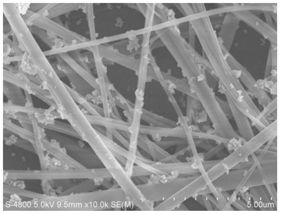
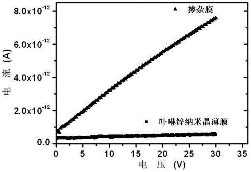
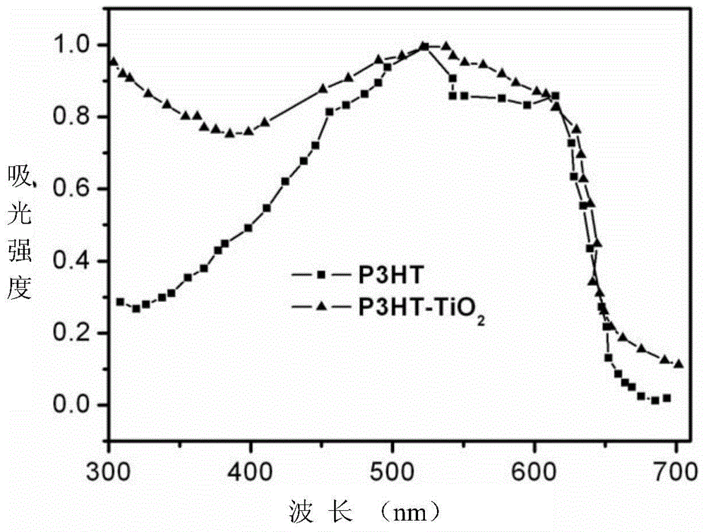

Image

  • Hybrid membrane production method
  • Hybrid membrane production method
  • Hybrid membrane production method

Examples


Embodiment 1

[0037] In the hybrid film of this embodiment, the organic semiconductor material in the raw material is zinc porphyrin, the first solvent is chloroform and octane, and the ratio of chloroform and octane is 4:1; the inorganic nanomaterial is zinc oxide, and the second solvent is ethanol .

[0038] The preparation method of this hybrid film comprises the following steps:

[0039] Step 1: Dissolve zinc porphyrin in the mixture of chloroform and octane to form the first mixture with a concentration of zinc porphyrin of 1 mg / mL; disperse zinc oxide in ethanol and disperse evenly by ultrasonic to form a zinc oxide concentration of 0.5 mg / mL of the second mixture. Among them, the solubility of porphyrin zinc in different solvents is different, and it affects the quality of subsequent nanocrystal assembly ability. Those skilled in the art know that for metal phthalocyanine compounds or metal porphyrin compounds themselves, the solubility in organic solvents is not high, so in order ...

Embodiment 2

[0045] In the hybrid film of this embodiment, the organic semiconductor material is cobalt octamethylporphyrin, the first solvent is chlorobenzene; the inorganic nano material is titanium dioxide, and the second solvent is water.

[0046] Step 1: dissolving cobalt octamethylporphyrin in the chlorobenzene mixture to form the first mixture with a cobalt octamethylporphyrin concentration of 2 mg / mL; disperse titanium dioxide in distilled water and disperse evenly by ultrasonic to form a concentration of titanium dioxide of 0.2 mg / mL of the second mixture.

[0047] Step 2: Transfer the first mixture to the inert substrate SiO by spin coating 2 On the substrate, let stand at room temperature for 40 minutes, and then anneal at 120° C. for 30 minutes, and form cobalt octamethylporphyrin cobalt nanocrystals after the chlorobenzene volatilizes. Wherein, the annealing treatment in this step is to allow the chlorobenzene solvent to evaporate faster and clean.

[0048] Step 3: Soak the ...

Embodiment 3

[0050] In the hybrid film of this embodiment, the organic semiconductor material in the raw material is perylene imide, the first solvent is chloroform and methanol, and its volume ratio is about 1:5; the inorganic nanomaterial is silver nanoparticles, and the second solvent is ethanol.

[0051] Step 1: dissolving peryleneimide in a mixture of chloroform and methanol to form the first mixture with a peryleneimide concentration of 0.2 mg / mL; dispersing silver nanoparticles in ethanol and ultrasonically dispersing them uniformly to form silver nanoparticles A second mixture at a concentration of 0.5 mg / mL. For compounds such as perylene imide or its derivatives, adjusting its concentration in the first mixture within the range of 0.1-5 mg / mL can stably obtain a nanocrystalline film structure.

[0052] Step 2: Transfer the first mixture to an inert substrate polyethylene terephthalate (PET) substrate by aerosol spray printing, and let it stand at room temperature for 30 minutes, ...


PUM


Abstract

The invention relates to a semiconductor material production technology, in particular to a hybrid membrane production method. The hybrid membrane production method includes the following steps: dissolving an organic semiconductor material in a first solvent to form a first mixture with concentration of 0.01-20mg/mL; dispersing an inorganic nano material into a second solvent to form a second mixture with concentration of 0.01-10mg/mL; transferring the first mixture onto an inert substrate for standing, and forming an organic semiconductor nanocrystalline after evaporation of the first solvent; transferring the second mixture onto the surface of the organic semiconductor nanocrystalline, performing annealing treatment and obtaining a hybrid membrane made of organic-inorganic materials after evaporation of the second solvent. The production method is simple to operate without rigid environments of high temperature and high vacuum, compatible with printed electronics processing methods such as ink-jet printing and aerosol jet printing, short in production cycle, low in cost and suitable for large-area mass production.

Description

technical field [0001] The invention relates to a semiconductor material preparation technology, in particular to a preparation method of an organic-inorganic hybrid film. Background technique [0002] Organic semiconductor materials have attracted great interest in recent years due to their unique optoelectronic properties. In particular, with the development of solution processing in recent years, organic semiconductor materials have shown incomparable advantages in the preparation of low-cost, large-area semiconductor devices. At the same time, the good flexibility of organic semiconductor materials makes them have important applications in the field of foldable and light-weight organic optoelectronic devices. Although great progress has been made in the preparation of organic optoelectronic materials and their application in optoelectronic devices, the low mobility and narrow spectral absorption of organic semiconductor materials are still important factors that limit t...

Claims


Application Information

Patent Timeline
IPC IPC(8): H01L51/00B82Y30/00B82Y40/00
Inventor 王凤霞潘革波
Owner SUZHOU INST OF NANO TECH & NANO BIONICS CHINESE ACEDEMY OF SCI
Why Eureka
Try Eureka