Noble metal nanostructure as well as preparation method and application thereof
A nanostructure and noble metal technology, applied in the direction of nanotechnology, nanotechnology, nanotechnology for materials and surface science, etc., can solve the problems of large particle size and uneven size, achieve uniform size and shape, and prepare The effect of simple process and pure gold nanostructure system
- Summary
- Abstract
- Description
- Claims
- Application Information
AI Technical Summary
Problems solved by technology
Method used
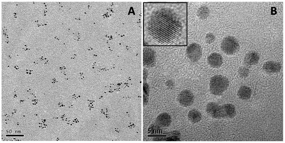
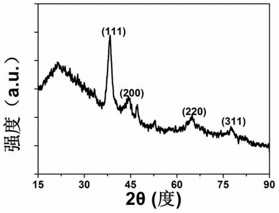
Image

Examples
preparation example Construction
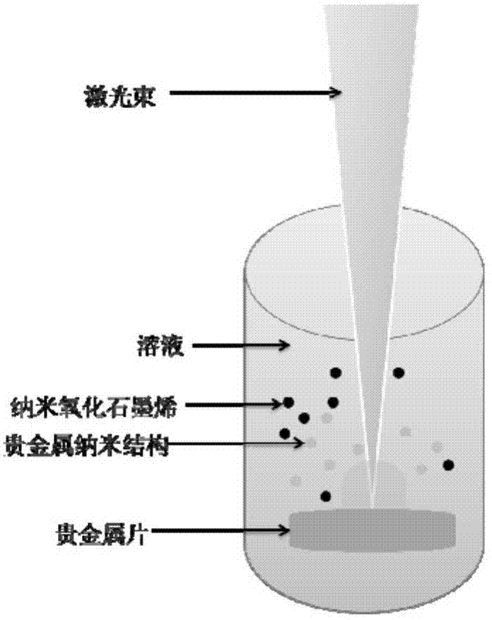
[0051] The method for preparing gold nanostructure provided by the invention comprises the following steps:
[0052] (1) Provide a precious metal sheet, and perform mechanical polishing on it, and place it in a reaction vessel;
[0053] (2) Inject the nano-graphene oxide solution into the reaction vessel, and the liquid level of the solution is not over the precious metal sheet;
[0054](3) The pulsed laser passes through the reaction vessel and the nano-graphene oxide solution, focuses on the surface of the precious metal sheet, and ablate the precious metal sheet;
[0055] (4) The solution in the reaction vessel is separated through a microporous membrane, and then the nanometer graphene oxide particles are removed by dialysis through a dialysis bag.
[0056] in, figure 1 A schematic diagram of obtaining noble metal nanostructures by liquid-phase pulsed laser ablation under the action of a nano-graphene oxide seed promoter provided by the present invention.
Embodiment 1
[0058] A method for preparing a gold nanostructure, comprising the steps of:
[0059] (1) Provide a gold flake, perform mechanical polishing, and place it in a reaction vessel; the purity of the gold flake is ≥99.99wt%; the thickness of the gold flake is 1mm;
[0060] (2) injecting the nano graphene oxide solution that concentration is 200mg / L into the reaction vessel, and the liquid level has not crossed the gold flake; the nano graphene oxide is a seed promoter; the particle diameter of the nano graphene oxide is 1~ 2nm;
[0061] (3) Provide a pulse laser generating device, guide the laser generated by it into the reaction container through the optical path conversion device, and focus on the surface of the gold sheet, and ablate the gold sheet;
[0062] The pulsed laser generating device is a Nd:YAG pulsed laser, the excitation wavelength is 532nm, and the pulse frequency is 10Hz; the laser energy is adjusted by adjusting the voltage of the pulsed laser generating device, ...
Embodiment 2
[0068] A method for preparing a gold nanostructure, comprising the steps of:
[0069] (1) Provide a gold flake, perform mechanical polishing, and place it in a reaction vessel; the purity of the gold flake is ≥99.99wt%; the thickness of the gold flake is 1mm;
[0070] (2) injecting the nano-graphene oxide solution that concentration is 40mg / L into reaction vessel, and the liquid level has not crossed described gold flake; Described nano-graphene oxide is seed promoter; The particle diameter of nano-graphene oxide is 1~ 2nm;
[0071] (3) Provide a pulse laser generating device, guide the laser generated by it into the reaction container through the optical path conversion device, and focus on the surface of the gold sheet, and ablate the gold sheet;
[0072] The pulsed laser generating device is a Nd:YAG pulsed laser, the excitation wavelength is 532nm, and the pulse frequency is 10Hz; the laser energy is adjusted by adjusting the voltage of the pulsed laser generating device,...
PUM
| Property | Measurement | Unit |
|---|---|---|
| Thickness | aaaaa | aaaaa |
| Particle size | aaaaa | aaaaa |
| Wavelength | aaaaa | aaaaa |
Abstract
Description
Claims
Application Information
PatSnap Eureka turns technology decisions into work you can execute. Powered by our Innovation Knowledge Graph, it runs expert workflows across engineering, life sciences, materials and intellectual property. Get your review-ready output in minutes.


