

White-light light emitting diode and preparation method thereof
A technology of light-emitting diodes and white light, applied in semiconductor devices, electrical components, circuits, etc., can solve the problems of complex composition of phosphors, poor color temperature uniformity, high ratio requirements, etc., achieve no ultraviolet environment, friendly, easy to operate at low cost , the effect of low color temperature
- Summary
- Abstract
- Description
- Claims
- Application Information
AI Technical Summary
Problems solved by technology
Method used
Image

Examples
preparation example Construction
[0048] The preparation method of the white light emitting diode of the present invention comprises the following steps:
[0049] Step 1. Take the n-type gallium nitride substrate for cleaning, use acetone, alcohol and deionized water to clean in sequence under ultrasonic, and finally put it in an oven to dry.
[0050] Step 2. uniformly sputtering gold particles on the n-type gallium nitride film as a catalyst for the reaction;
[0051] Step 3. prepare antimony oxide, zinc oxide, carbon powder mixed sample as reactant;
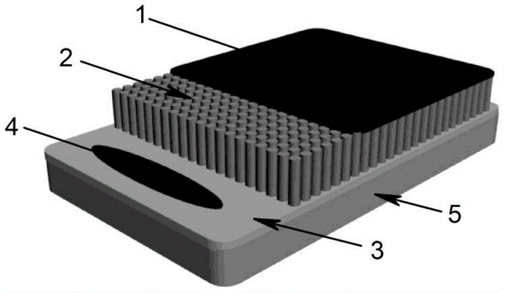
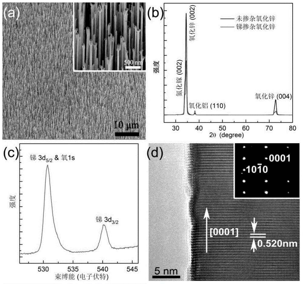
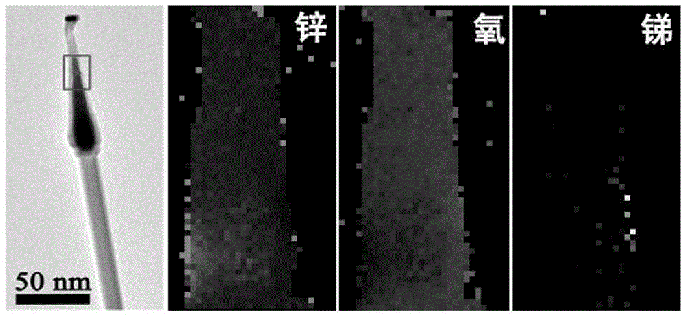
[0052] Step 4. Take the mixed sample in step 3 and put it into a quartz boat, put the reaction substrate into a quartz glass tube, put the two into a low-temperature furnace for chemical vapor deposition reaction, and grow antimony-doped p ZnO nanowire arrays to form heterojunctions;
[0053] Step 5. Use metal indium and antimony doped p-type zinc oxide nanowire array top contacts as positive electrodes;
[0054] Step 6. Use the indium gold electrode and the...
Embodiment 1
[0059] In this embodiment, the preparation method of white light emitting diodes includes the following steps:
[0060] 1) Reaction substrate cleaning and preparation of raw materials
[0061] Cut the n-type gallium nitride wafer into a square of 5mm*5mm uniform size, put it into a beaker, and then ultrasonically clean it in acetone solution at 50°C for 15 minutes, then in ethanol solution at room temperature for 10 minutes, and repeat in high-purity deionized water. Ultrasound, 2 minutes each time, after the substrate is cleaned, put it into a clean oven for drying to obtain a clean reaction substrate.
[0062] Then prepare the raw materials for the reaction, put the zinc oxide powder and carbon powder in a mass ratio of 1:1, and the molar ratio of zinc oxide and antimony oxide powder in a 1:1 / 20, put the three powders into a beaker, pour the ethanol solution, and put the magnet , Use a heating magnetic stirrer to heat and stir to form a slurry, put the powder slurry into a ...
Embodiment 2
[0077] In this embodiment, the preparation method of white light emitting diodes includes the following steps:
[0078] 1) Reaction substrate cleaning and preparation of raw materials
[0079] In this example, the difference between the cleaning of the reaction substrate and that of Example 1 is that the substrate is treated with hydrochloric acid, soaked at room temperature for 48 hours, and then repeatedly ultrasonically cleaned with deionized water and dried. The raw materials of zinc oxide powder and antimony oxide powder The proportioning molar ratio becomes 1:1 / 10, and other parameters remain unchanged.
[0080] 2) Growth of Sb-doped ZnO nanowire arrays
[0081] In this example, the difference from Example 1 is that 0.3 g of mixed powder is taken, the reaction temperature is changed to 950° C., and other conditions remain unchanged.
PUM
 Abstract
Description
Claims
Application Information