Method for fast preparing high-temperature service total IMC microscale solder joint through multi-layer micron and submicron film

A high-temperature service and multi-layer film technology, applied in the field of micro-connection, can solve problems such as low production efficiency, inability to achieve precise control of joint components, and difficulty in large-scale industrial application, so as to achieve stable performance and promote large-scale industrial applications. The effect of shortening the time

Active Publication Date: 2015-08-26
HARBIN INST OF TECH
View PDF7 Cites 10 Cited by
  • Summary
  • Abstract
  • Description
  • Claims
  • Application Information

AI Technical Summary

Problems solved by technology

However, if an all-IMC solder joint with a size of ten microns or larger is prepared, the reaction time needs to be at least tens of minutes, the production efficiency is too low, and the composition of the joint cannot be precisely controlled, making it difficult to achieve large-scale industrial application

Method used


Image

  • Method for fast preparing high-temperature service total IMC microscale solder joint through multi-layer micron and submicron film

Examples


Embodiment 1

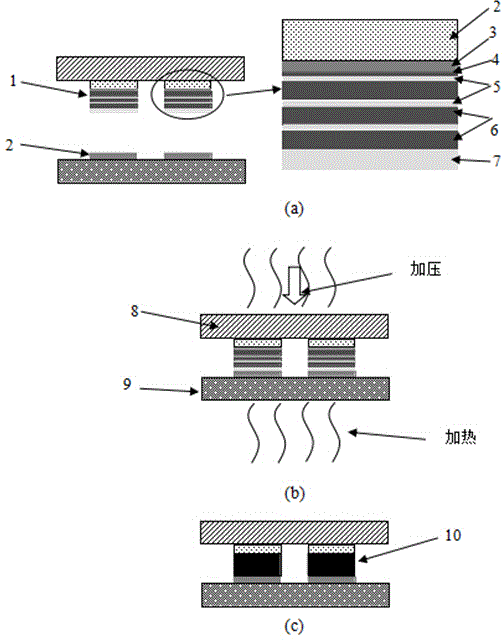
[0031] Such as figure 1 As shown, Cu 3 The Sn full IMC micro-soldering method comprises the steps:

[0032] Step 1: Prepare corresponding openings on the photoresist film by photolithography in the area of ​​the bonding pad on the chip surface. The area of ​​the pad and the size of the photoresist opening are 300 microns × 300 microns, and the height of the photoresist is 12.0 Microns.

[0033] Step 2: A Cu film is prepared on the bonding pad area of ​​the chip by an evaporation method, and the thickness of the film layer is 2.0 microns.

[0034] Step 3: An electroplating method is used to prepare a Sn film on the surface of the Cu film in the previous step, and the thickness of the film layer is 0.8 microns.

[0035] Step 4: Deposit Cu on the surface of the Sn film in the previous step by vapor deposition. The thickness of the deposited film is prepared according to the atomic molar ratio of the Cu film to the previous layer of Sn film slightly less than 3:1, and the thick...

Embodiment 2

[0042] Such as figure 1 As shown, the rapid preparation of Ag by multilayer micron and submicron films 3 The Sn full IMC micro-soldering method comprises the steps:

[0043] Step 1: Prepare a mask plate by laser etching. The opening area of ​​the mask corresponds to and aligns with the pad area to be bonded to the wafer. The area of ​​the pad and the size of the mask opening are 200 microns × 200 microns. The mask The thickness is 15.0 microns.

[0044] Step 2: A sputtering method is used to prepare an Ag film on the pad area of ​​the wafer, and the thickness of the film layer is 3.0 microns.

[0045] Step 3: Preparing a Sn film on the surface of the Ag film in the previous step by evaporation method, the thickness of the film layer is 0.5 micron.

[0046] Step 4: Depositing Ag on the surface of the Sn film in the previous step by sputtering, the thickness of the deposited film layer is prepared according to the atomic molar ratio of the Ag film to the previous Sn film bein...


PUM

PropertyMeasurementUnit
thicknessaaaaaaaaaa
thicknessaaaaaaaaaa
thicknessaaaaaaaaaa

Abstract

A method for fast preparing a high-temperature service total IMC microscale solder joint through a multi-layer micron and submicron film comprises the following steps that a Cu or Ag film is prepared on the surface of a bonding pad of a wafer or a chip, Sn/(Cu or Ag) with the micron-level or submicron-level thickness is sequentially deposited, the deposition step of the Sn/(Cu or Ag) film can be repeatedly executed according to the height of the needed solder joint, and after the needed thickness is reached, a Sn film is prepared on the surface of the multi-layer micron and submicron film; a multi-layer film structure of the wafer or the chip is aligned with a connecting bonding pad needed by a substrate or other wafers or other chips, and pressure is applied; the system is placed in a reflow oven, the preheating stage, the insulating stage, the reflowing stage and the cooling stage are carried out, and finally preparation of the total IMC solder joint is achieved. The total IMC solder joint preparing technology can be well compatible with a traditional brazing filler metal reflow soldering technology or a hot pressure soldering technology, and preparation of the IMC solder joint at the low temperature and within the short time can be achieved. The low-temperature bonding high-temperature service of the solder joint is achieved on the premise that cost is low, and the production efficiency is high.

Description

technical field [0001] The invention belongs to the field of micro-connection technology, and relates to a method for interconnecting wafers or chips and substrates, wafers or chips and other wafers or chips in electronic devices, components, or microsystems, and specifically relates to a method for interconnecting wafers or chips with other wafers or chips. The rapid and low-temperature preparation of micron and submicron films can realize the method of all-intermetallic compound (Intermetallic Compounds-IMC) micro-soldering joints in high-temperature service. Background technique [0002] Connection technology is one of the core technologies to realize the packaging of electronic components or components, the packaging of micro-electromechanical systems (MEMS), and the three-dimensional packaging of wafers. With the development of electronic systems in the direction of high performance, high power, and high density, the heat generation of electronic systems will increase s...

Claims


Application Information

Patent Timeline
Patent Type & Authority Applications(China)
IPC IPC(8): C23C28/02C23C14/04
Inventor 刘威王春青田艳红
Owner HARBIN INST OF TECH
Why Eureka
Try Eureka