Transparent conducting thin film with enhanced thermal stability and preparation method and application thereof

A technology of transparent conductive film and thermal stability, applied in the direction of conductive layer on insulating carrier, semiconductor/solid-state device manufacturing, circuit, etc., can solve problems such as inability to completely overcome condensation phenomenon, unsatisfactory stability, complex structure, etc., to achieve Reduce the amount of silver material, improve battery efficiency and stability, and improve the effect of energy level matching

Active Publication Date: 2015-10-14
SHANGHAI UNIVERSITY OF ELECTRIC POWER
View PDF4 Cites 30 Cited by
  • Summary
  • Abstract
  • Description
  • Claims
  • Application Information

AI Technical Summary

Problems solved by technology

In the transparent conductive film of this invention, a semiconductor thin layer that inhibits the diffusion of atoms in the metal layer to the oxide layer is formed at the interface between the oxide layer and the metal layer by inserting the suppression layer. However, the invention does not disclose the use of alloy layers, and simply

Method used


Image

  • Transparent conducting thin film with enhanced thermal stability and preparation method and application thereof
  • Transparent conducting thin film with enhanced thermal stability and preparation method and application thereof
  • Transparent conducting thin film with enhanced thermal stability and preparation method and application thereof

Examples


Embodiment 1

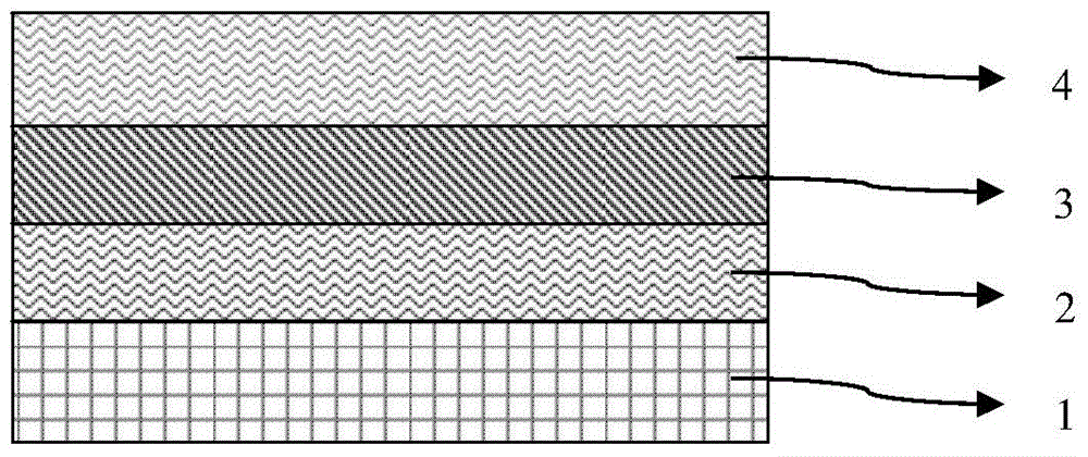
[0030] A kind of transparent conductive film based on silver alloy layer, its cross-sectional schematic diagram is as follows figure 1 As shown, it consists of a substrate 1, a first semiconductor layer 2, a silver alloy layer 3 and a second semiconductor layer 4 from bottom to top;

[0031] The material of the substrate 1 is glass with a thickness of 1mm;

[0032] The material of the first semiconductor layer 2 is GZO with a thickness of 40nm;

[0033] The material of the silver alloy layer 3 is silver (AgAl), and the thickness is 12nm;

[0034] The material of the second semiconductor layer 4 is GZO with a thickness of 50nm.

[0035] The above-mentioned preparation method of a transparent conductive film based on silver aluminum alloy layer, the specific steps are as follows:

[0036] Use cleaned transparent glass, place it in the cavity of the magnetron sputtering system, and evacuate it to a vacuum of 10 -5 Torr, followed by Ar gas, sputtering the first semiconductor l...

Embodiment 2

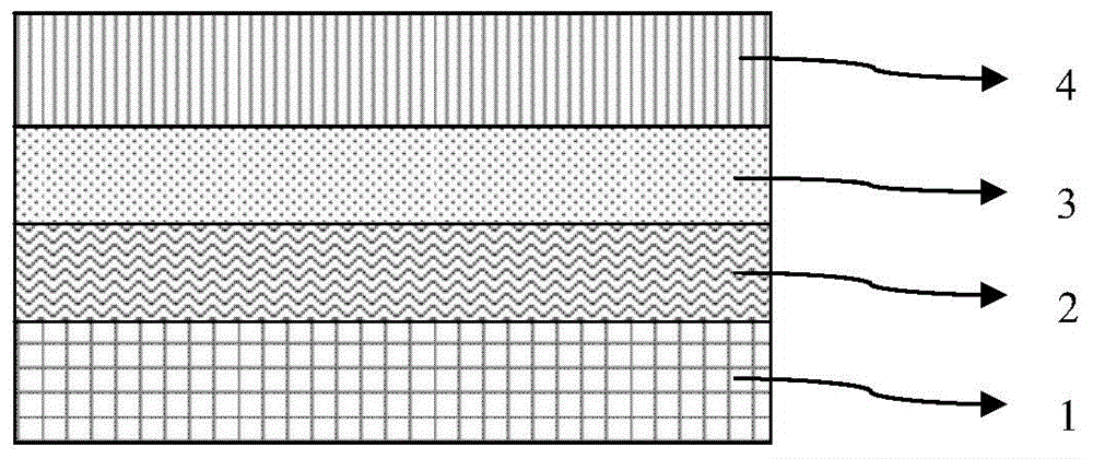
[0039]A kind of transparent conductive film based on silver alloy layer, its cross-sectional schematic diagram is as follows figure 2 As shown, it consists of a substrate 1 , a first semiconductor layer 2 , a silver alloy layer 3 and a second semiconductor layer 4 from bottom to top.

[0040] The material of the substrate 1 is glass with a thickness of 1mm;

[0041] The material of the first semiconductor layer 2 is MoO 3 , with a thickness of 10nm;

[0042] The material of the silver alloy layer 3 is AgAl with a thickness of 12nm;

[0043] The material of the second semiconductor layer 4 is MoO 3 , thickness 50nm.

[0044] The above-mentioned preparation method of a transparent conductive film based on silver aluminum alloy, the specific steps are as follows:

[0045] Use cleaned transparent glass, place it in the cavity of the vacuum thermal evaporation system, and evacuate it to a vacuum of 5*10 -6 Torr, and then the first semiconductor layer MoO was plated respectiv...

Embodiment 3

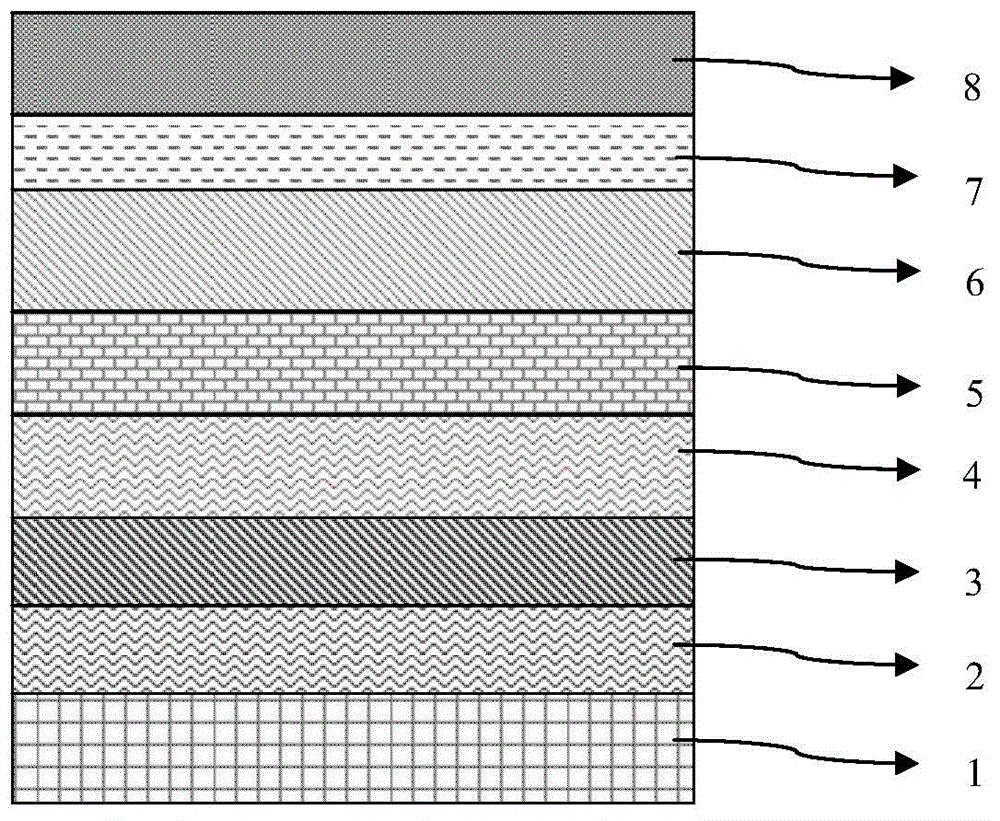
[0048] Such as image 3 As shown, the transparent conductive thin film structure obtained in Example 1 is applied to an organic solar cell, including 1 glass substrate, 2 first semiconductor layer GZO, 3 silver metal layer AgAl, 4 second semiconductor layer GZO, 5 Electron transport layer ZnO, 6 organic photoactive layers, 7 hole transport layer MoO 3 , 8 battery anode Ag. A single specific material is given in this embodiment, which does not limit the choice of other materials, but is just an example to illustrate the present invention. The transparent conductive film based on the silver-aluminum alloy layer is deposited by magnetron sputtering, then spin-coated with a 30nm ZnO electron transport layer 5, and after annealing at 140 degrees, then spin-coated with a PCE10:PC70BM (ratio 1:1.5) photoactive layer 6, followed by vacuum thermal evaporation of 8nm MoO 3 A hole transport layer 7 and an anode 8 of 100 nm silver layer. The efficiency of the organic solar cell adopti...


PUM

PropertyMeasurementUnit
Thicknessaaaaaaaaaa
Thicknessaaaaaaaaaa
Thicknessaaaaaaaaaa

Abstract

The invention relates to a transparent conducting thin film with enhanced thermal stability and a preparation method and application thereof. The transparent conducting thin film consists of a substrate, a first semiconductor layer, a silver alloy layer and a second semiconductor layer sequentially from bottom to top; according to the silver alloy layer, metal silver is combined with aluminum, zinc, titanium, copper, magnesium, nickel, rare earth elements or chromium to form a bi-element silver alloy layer or a multi-element silver alloy layer. The transparent conducting thin film provided by the invention can be used for photoelectric devices, such as organic light-emitting devices (OLEDs), organic solar cells and perovskite batteries; furthermore, on the basis of improving the thermal stability of the photoelectric devices, the dose of the photoelectric devices on a silver material per unit area can be reduced, device cost can be beneficially controlled, resources are saved; and the transparent conducting thin film also can be applied to magnetic shielding, special functional window coatings, transparent heat preservation building glass and the like.

Description

technical field [0001] The invention belongs to the field of photoelectric devices, and in particular relates to a transparent conductive film with enhanced thermal stability, a preparation method and application thereof. Background technique [0002] Transparent conductive oxides (TCOs) usually have the characteristics of wide band gap, high light transmittance and low resistivity, and have a wide range of applications in the fields of flat-panel displays, solar cells, electromagnetic shielding, and special function window coatings. At present, transparent conductive films such as tin-doped indium oxide (ITO), fluorine-doped tin oxide (FTO), gallium-doped ZnO (GZO) and aluminum-doped ZnO (AZO) have been widely used in the field of optoelectronics, but they have poor flexibility. Can not meet the application requirements of flexible devices. Semiconductor layer|metal layer|semiconductor layer (SMS) structure transparent conductive film developed in recent years such as ITO|...

Claims


Application Information

Patent Timeline
IPC IPC(8): H01B5/14H01L51/44
CPCY02B10/10Y02E10/549
Inventor 周建萍
Owner SHANGHAI UNIVERSITY OF ELECTRIC POWER
Why Eureka
Try Eureka